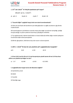
NT 502: Micro/Nanofabrication
This course covers i) the fundamentals of shaping materials at micro and nanoscale (e.g,
diffusion, etching, and oxidation), ii) lithography, material deposition, pattern transfer, and
metrology, iii) charged particles lithography (e.g., e-beam and focused ion beam
lithography), iv) scanning probe microscopy-based fabrication techniques (e.g., dip-pen
nanolithography and nanografting), v) nanoimprint lithography and step-and-flash
lithography, vi) unconventional fabrication techniques (e.g., nanoskiving and nanosphere
lithography), vii) self-assembly, templated/directed self-assembly and soft-lithography, viii)
bulk and surface micromachining, and ix) 3D printing. The course will also pay specific
attention to the applications of micro/nanofabricated devices.
NT 502: Mikro/Nanofabrikasyon
Bu dersin içeriği i) malzemeleri mikro ve nanoboyutta şekillendirmenin temelleri (difüzyon,
dağlama ve oksidasyon), ii) litografi, malzeme depozitleme, patern transferi ve metroloji, ii)
şarjlı parçacık litografisi (e-ışını ve fokuslanmış iyon ışını litografisi), iv) taramalı uç
mikroskopisi-temelli üretlim teknikleri (batırmalı uç litografisi ve nanograftlama), v)
nanobaskılama litografisi ve adım-ve-flaş litografisi, vi) konvensiyonel olmayan üretim
teknikleri (nanoskiving ve nanoküre litografisi), vii) öztoplanma, kalıplı/güdümlü öztoplanma
ve yumuşak litografi, viii) gövde ve yüzey mikroimalatı ve ix) 3D baskılamadır. Bu ders
mikro/nano yöntemlerle üretilmiş aletlerin uygulamalarına da özel önem verecektir.
Session 1: Ozge Akbulut (February 7th, 9:30–12:30)
i)
ii)
iii)
Introduction to the course
Electronic properties of conductors, semiconductors, and insulator (e.g., band
structure, Fermi level, Fermi Function, Ohm’s Law)
Properties of commonly used polymers, semiconductors and metals in
micro/nanofabrication
Session 2: Cem Ozturk (February 7th, 13:30–16:30)
i)
Optical lithography (projection systems, resolution vs DRAM half-pitch, technology
nodes 193i technology, and computational enhancements)
Session 3: Cem Ozturk (February 14th, 9:30–12:30)
i)
Commercial applications of micro/nanofabrication (e.g., CMOS, BiCMOS, RFIC,
and MEMS/NEMS
Session 4: Volkan Ozguz (February 7th, 13:30–16:30)
i)
Fundamentals of shaping materials at nanoscale
a) Diffusion
b) Etching
c) Oxidation
d) Ion implantation
Session 5: Ali Koşar (February 21th, 9:30–12:30)
i)
Bonding and packaging
Session 6: Onur Serbest (February 21th, 13:30–16:30)
i)
ii)
SUNUM Safety Training
Laboratory session in SUNUM Clean Room
Session 7: Bahattin Koc (February 28th, 9:30–12:30)
i)
ii)
Additive manufacturing
Printing of nanocomposites
Session 8: Meltem Sezen/Cenk Yanik (February 28th, 13:30–16:30)
i)
ii)
Focused ion beam lithography (with laboratory)
E-beam lithography (with laboratory)
Session 9: Ozge Akbulut (March 7th, 9:30–12:30)
i)
ii)
Nanoimprint Lithography (NIL)
Step-and-flash Lithography (SFIL)
Session 10: Ozge Akbulut (March 7th, 13:30–16:30)
i)
Unconventional fabrication techniques (e.g.,nanoskiving, nanosphere projection
lithography)
Session 11: Erhan Budak (March 14th, 9:30–12:30)
i)
Micromachining
Session 12: Gozde Ince (March 14th, 13:30–16:30)
i)
Scanning probe microscopy-based fabrication techniques
Section 13: Fevzi Cakmak Cebeci (March 21st, 9:30–12:30)
i)
ii)
Self-assembly, templated/directed self-assembly
Soft lithography
Session 14: Student presentations (March 21st, 13:30–16:30)
© Copyright 2026 Paperzz