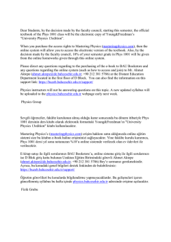
ボーズ凝縮原子を用いた量子原子光学の研究 課題番号:17340120 平成 17-19 年度科学研究費補助金 基盤研究 B 研究成果報告書 平成 20 年 4 月 研究代表者:中川賢一 (電気通信大学レーザー新世代研究センター准教授) 平成 17-19 年度科学研究費補助金 基盤研究 B ボーズ凝縮原子を用いた量子原子光学の研究 課題番号:17340120 研究組織 研究代表者 中川賢一(電気通信大学レーザー新世代研究センター准教授) 研究費 平成 17 年度 7,100 千円 平成 18 年度 4,900 千円 平成 19 年度 3,100 千円 15,100 千円 計 研究発表 論文 1. Munekazu Horikoshi and Ken'ichi Nakagawa, Suppression of dephasing due to a trapping potential and atom-atom interactions in a trapped-condensate interferometer, Phys. Rev. Lett. 99, 180401 (2007). 2. Mark Sadgrove, Munekazu Horikoshi, Tetsuo Sekimura1 and Ken'ichi Nakagawa, Coherent control of ballistic energy growth for a kicked Bose-Einstein condensate, Eur. Phys. J. D 45, 229-234 (2007). 3. Mark Sadgrove, Munekazu Horikoshi, Tetsuo Sekimura, and Ken'ichi Nakagawa , Rectified momentum transport for a kicked Bose-Einstein condensate, Phys. Rev. Lett. 99, 043002 (2007). 4. Munekazu Horikoshi, Ken'ichi Nakagawa, Dephasing due to atom-atom interaction in a waveguide interferometer using a Bose-Einstein condensate, Phys. Rev. A 74, 031602(R) (2006). 5. Munekazu Horikoshi, Ken'ichi Nakagawa, Atom Chip based fast production of Bose-Einstein condensate, Appl. Phys. B 82, 363-366 (2006). 6. K. Nakagawa, Y. Suzuki, M. Horikoshi, and J. B. Kim, Simple and efficient magnetic transport of cold atoms using moving coils for the production of Bose-Einstein condensation, Appl. Phys. B 81, 791-794 (2005). 国際会議発表 1. Ken'ichi Nakagawa, Munekazu Horikoshi : Bose-Einstein-Condensate Interferometer on an Atom Chip with a Long Coherence Time, 18th International Conference on Laser Spectroscopy (ICOLS), Telluride, Colorado, June 25-29 (2007). 2. Ken'ichi Nakagawa and Munekazu Horikoshi : Atomic interferometer on an atom chip (invited), International Conferernce on Lasers and Nanomaterials (ICLAN), Kolcata, Nov. 30 - Dec. 2 (2006). 3. M. Horikoshi, Y. Suzuki, K. Nakagawa : Fast and Efficient Production of Bose-Einstein Condensate Atoms based on an Atom Chip, International Quantum Electronics Conference 2005, Tokyo, July 11-15 (2005). 4. K. Nakagawa, M. Horikoshi : Towards coherent atom optics in an atom waveguide, 14th International Laser Physics Workshop, Kyoto, July 4-8 (2005). 5. Ken'ichi Nakagawa, Munekazu Horikoshi, Yusuke Koda : Atomic interferometer with cold rubidium atoms for the precision measurements of gravirational acceleration, 17th International Conference on Laser Spectroscopy, Scotland, June 19-24 (2005). 6. Munekazu Horikoshi, Ken'ichi Nakagawa : Atom-chip-based fast production of Bose-Einstein condensate atoms, 17th International Conference on Laser Spectroscopy, Scotland, June 19-24 (2005). 国内学会発表 1. 福泉美穂、玉木嘉人、桂川眞幸、中川賢一:87Rb 原子の二光子遷移によるリュー ドベルグ状態の分光 II、日本物理学会第 63 回年次大会、23aQD-8, 2008 年 3 月. 2. Phase defects in an optical lattice: effect on coherent atomic dynamics, 日本物 理学会第 63 回年次大会、25pQD-7, 2008 年 3 月. 3. 少数個レーザー冷却 Rb 原子における Rydberg 励起の双極子ブロッケード、日本 物理学会第 63 回年次大会、26aQD-1, 2008 年 3 月. 4. Mark Sadgrove, Munekazu Horikoshi, Tetsuo Sekimura, Ken'ichi Nakagawa : Bose-Einstein Condensates in pulsed optical lattices, 日本物理学会第 62 回年 次大会、22pRG-1, 2007 年 9 月. 5. 関邨哲雄、杉江宏太、中川賢一:Rb 原子の 2 波長光双極子トラップ、日本物理 学会第 62 回年次大会、24pRH-8, 2007 年 9 月. 6. 福泉美穂、玉木嘉人、Mark Sadgrove、中川賢一:87Rb 原子の二光子遷移による リュードベルグ状態の分光、日本物理学会第 62 回年次大会、 21pRH-13, 2007 年 9 月. 7. Mark Sadgrove、堀越宗一、関邨哲雄、中川賢一:Shift in fundamental quantum resonance for atoms in a pulsed optical lattice、日本物理学会 2007 年春季大会、 20aXK11, 2007 年 3 月. 8. 堀越宗一、中川賢一:長いコヒーレンス時間を持った調和ポテンシャル中での BEC 干渉計、日本物理学会 2007 年春季大会、20aXK10, 2007 年 3 月. 9. 中川賢一、江村真史、後藤亮彦:電場を用いたアトムチップによるボーズ凝縮体 の操作 II、日本物理学会 2007 年春季大会、 20aXK9, 2007 年 3 月. 10. 玉木嘉人、Mark Sadgrove、中川悠輔、中川賢一:単一原子トラップを用い た単一光子源、日本物理学会 2007 年春季大会、19aXK10, 2007 年 3 月. 11. 堀越宗一、中川賢一:磁場ガイド BEC 干渉計における位相シフトとコントラ スト低下、日本物理学会第 61 回年次大会、29pTA12, 2006 年 3 月. 12. 江村真史、堀越宗一、中川賢一:電場を用いたアトムチップによるボーズ凝 縮体の操作、日本物理学会第 61 回年次大会、29pTA11, 2006 年 3 月. 13. 後藤亮彦、豊永匡利、中川賢一:フェルミ縮退に向けての 40K と 87Rb の同時 トラップ、日本物理学会第 61 回年次大会、28aRE11, 2006 年 3 月. 14. 小田悠介、後藤亮彦、中川賢一:原子干渉計を用いた重力加速度測定Ⅲ、日 本物理学会 2005 年秋期大会、 20aWA14, 2005 年 9 月. 15. 中川悠輔、中川賢一:磁気光学トラップによる 単一原子トラップⅡ、日本物 理学会 2005 年秋期大会、19aWA2, 2005 年 9 月. 16. 堀越宗一、江村真史、中川賢一:磁場ガイド中のボース凝縮体の操作、日本 物理学会 2005 年秋期大会、19aWA3, 2005 年 9 月. 研究会発表等 1. 中川賢一:アトムチップによるボース凝縮原子の操作とその応用、原子・分子・ 光科学(AMO)第3回討論会、招待講演、東大駒場、2006 年 6 月 16 日. 2. 中川賢一:光でつくるコヒーレントな原子、2007 年度日本物理学会科学セミナー、 電気通信大学、2007 年 8 月 24 日. 目次 1. はじめに 1 2. アトムチップを用いた高速 BEC 生成装置の開発 3 3. アトムチップ上の BEC 干渉計 7 4. BEC 原子を用いた量子ラチェット効果 13 5. 単一原子トラップの開発 16 6. 電場・磁場ハイブリッド型アトムチップの開発 19 7. まとめ 22 参考文献 23 A 付録 25 A.1 原著論文 26 A.2 国際会議プロシーディング等 52 A.3 研究会資料等 62 1. はじめに レーザー冷却によって得られる温度 1μK 程度の極低温原子においてはそのド・ブ ロイ波長は 100nm 以上にもなり粒子としてよりも波としての性質が顕著に現れる。こ のような極低温原子の温度をさらに下げ、また原子密度を上げて隣り合う原子同士の 原子波が重なり合うようにすると多数の原子が全て同じ量子状態に落ち込むいわゆ るボース・アインシュタイン凝縮(Bose-Einstein Condensation: BEC)が実現される。こ のボース凝縮状態の原子は光におけるレーザーと同様に多数の原子の波動関数の位 相が揃ったコヒーレントな物質波とみなすことができ、このボース凝縮から取り出さ れた原子はレーザー光と同様に高い干渉性を示すため原子レーザーと呼ばれる。この ようなコヒーレントな物質波を光と同様に操作する研究はコヒーレント原子光学と 呼ばれ、1995 年に Cornell 等によって最初の原子のボース・アインシュタイン凝縮が 実現されて以来この分野の研究は劇的な発展を遂げてきた 1)。また最近では光におけ る量子光学と同様に原子の波動および粒子の二重性をフルに用いて非古典的な量子 状態を原子において実現する量子原子光学の研究が行われるようになり、これは光と 同様に量子コンピューターなどの量子情報処理への応用が期待されている 2)。 本研究はこのようなボース凝縮原子によるコヒーレントな物質波を用いた原子光 学の基礎技術および物理の確立およびこの様々な分野への応用をめざしたものであ る。本研究ではまず原子光学の研究において重要となるコヒーレントな物質波の発生 源であるボーズ凝縮原子の生成装置の開発を行った。アトムチップと呼ばれる集積化 原子回路の手法を用いたボース凝縮生成装置を開発し、従来より一桁以上高速にボー ス凝縮原子を生成することが可能になり、様々な原子光学実験を効率良く行うことを 可能にした。次にこのアトムチップを用いたボース凝縮生成装置を用いてチップ上で のボース凝縮原子を用いた原子干渉計の研究を行った。従来の自由空間中の原子に代 わってトラップされた原子を用いた原子干渉計が実現されれば重力による自由落下 に制限されずに長い相互作用時間が得られるため、高感度なジャイロスコープや加速 度センサーなどへの応用が期待されている 3),4) 。またボース凝縮原子を用いたコヒー レント原子光学の研究の一つとしてパルス状の光定在波ポテンシャル中の原子の運 動の研究を行った。この系は量子キック回転子と呼ばれ今までにレーザー冷却原子を 用いて実験において量子カオスの研究が行われてきたが本研究では単一の量子状態 にあるボース凝縮原子を用いることにより精密にこの系の性質を調べることが可能 になる。本研究ではボース凝縮原子を用いた量子キック回転子系において量子ラチェ ット効果の実現を予想してこれを実験によって実証した。近年注目されている量子コ ンピューターなどの量子情報処理を中性原子で行うためにはボース凝縮原子のよう なマクロな原子集団だけではなく、原子を 1 個レベルで操作する必要がある。このた 1 め本研究ではレーザー冷却原子を光双極子トラップ中に 1 個レベルでトラップおよび 検出するための基礎技術の開発を行った。この単原子操作および検出の技術を先のア トムチップによる原子回路の技術と組み合わせることにより原子の粒子性および波 動性を究極的に追求する量子原子光学の研究が可能になるとものと期待される。 2 2. アトムチップを用いた高速ボース凝縮原子生成装置の開発 アトムチップと呼ばれる基板上に集積化された原子回路を実現する方法が近年盛 んに研究されている 5)。これはリソグラフィー技術を用いて基板上に微細な電線パタ ーンを作成し、この電線に電流を流すことによって作られる微細な磁場ポテンシャル を用いて極低温原子を電線パターンに沿ってガイドして自由自在に操作しようとい うものである。このアトムチップを用いると原子を 1 個ずつトラップしたり操作する ことが可能になるため、中性原子を用いた量子コンピューターの実現という観点から 非常に興味が持たれている。またアトムチップ上の原子導波路によって極低温原子や ボース凝縮原子をガイドして光の干渉計と同様の原子干渉計が実現可能となり、光の 干渉計を超える高い感度のジャイロスコープや加速度計が実現可能になるものと期 待されている。 我々はこのアトムチップ上でボース凝縮原子を用いたコヒーレント原子光学の研 究を行うため、先ずアトムチップを用いたボース凝縮原子生成装置を開発した 6)。ア トムチップによって作られる微細な磁場ポテンシャルはボース凝縮の実現に必要な 高い原子密度を比較的容易に実現できることから高速で高効率な蒸発冷却が可能と なりボース凝縮原子の生成に好都合である。図 1(a)に本研究で作成したアトムチップ の基板を示す。基板材料としては絶縁体で電線からの発熱を効率良く放熱するため熱 伝導性が高いことが求められ、シリコン、サファイヤ、窒化アルミ(AlN)などが用い られる。電極材料としては電流による発熱を小さくするため電気伝導率が高い銅、金、 アルミなどが用いられる。本研究ではシリコン基板上にリソグラフィー技術を用いて 電線パターンのマスクを作成して金蒸着を行い、さらに金めっきを用いて電極の厚さ を 10μmまで増やした(図 1(b))。 (a) (b) (c) 原子導波路 原子 50~200μm Si 原子 ~100μm SiO2 金 銅 2 cm Bx 電線 電流 I Bϕ = μ0 I 2πr 図 1 アトムチップ。(a) アトムチップの基板。(b) 電極の構造。(c) 電線を流れる電流が作る 磁場による原子導波路。 3 このアトムチップ上の電線に電流を流すと電線の周りには円形の磁場 Bφ=μ0I/2πr が 生じるが、これに電線に垂直方向に一様な磁場 Bx を加えると電線の中心から距離 μ0I/2πΒx の位置で磁場がゼロになり原子を電線に沿って閉じ込める磁場ポテンシャル が作られ、スピンを持った原子を電線に沿ってガイドする原子導波路が実現される (図 1(c))。実際にはさらに電線に沿った方向にも磁場を加えて磁場の最小値がゼロで ないようにしてマヨナラ遷移による原子のスピンフリップを防ぐ。このように作られ る磁場ポテンシャルによってスピンを持つ原子は電線に沿ってその近くに強く閉じ 込められるため、電子回路と同様に原子を電線パターンに沿って操作して一種の原子 回路が実現される。様々な電線パターンを用いることにより電線に沿って閉じ込める 導波路以外にも 3 次元的に原子を閉じ込める 3D トラップ、またこれを一列に並べた アレー型トラップなども実現することができる(図 2)。 (a) 導波路 I (c) 1Dアレー型トラップ (b) 3Dトラップ 原子 電線 I B B 図 2 アトムチップ上の原子光学素子。(a) 導波路、(b) 3D トラップ、(c) 1D アレー型ト ラップ このようなアトムチップをガラスセル内 アトムチップ に配置して 磁場トラップ 用コイル 87 Rb 原子のボース凝縮原子を 生成する装置を実現した(図 3)。ガラスセル はイオンポンプおよびチタンサブリメンシ ョンポンプにより約 10-10 トル(10-9 Pa)以下 の超高真空に排気されている。先ずセル中 レーザー 光 Rb原子 MOT ガラス セル UV LED 温度約 100μΚ程度に冷却して磁気光学トラ ップに 107 個以上の冷却 Rb 原子を集める。 次にこの冷却 Rb 原子は磁場トラップに移 行され、複数の磁場トラップコイルを用い 4cm 図 3 の室温 Rb 原子をレーザー冷却法によって アトムチップを用いた小型・高速 て 2cm 上方のアトムチップの基板近くまで 輸送される。最後にアトムチップの電線に BEC 生成装置 4 電流を流してチップ上のマイクロ磁場ポテンシャルに原子がローディングされる(図 4)。チップにローディングされた冷却 Rb 原子は圧縮され、RF 磁場によるスピンフリ ップを用いた蒸発冷却を用いてさらに原子の温度を冷やす。温度が凝縮の相転移温度 約 2μK 程度まで下げると原子の速度分布に速度がほぼゼロの成分が現れてボース凝 縮が始まり、さらに温度を下げるとほぼ全ての原子が凝縮する(図 5)。 このようなアトムチップを用いた方法によりチップ上に最大 15000 個のボース凝縮 Rb 原子を 10 秒以内に生成することができる。これは従来の大型の磁場コイルを用い た磁場トラップによるボース凝縮生成に比べて生成される凝縮原子の個数は一桁程 度少ないが生成時間は 1/3 以下に短縮される。これはアトムチップで作られる微小な 磁場トラップにより高い原子密度が得られ、原子の弾性衝突確率を高くすることが可 能となり、蒸発冷却が高効率かつ高速に行われるためである。 10mm 基板 図 4 レーザー冷却 Rb 原子のアトムチップへのローディングの様子 サーマル原子 BEC サーマル原子+BEC 1.83MHz 1.86MHz 1.78MHz Nc=15000 N=50000 光学密度 0.6 T=2μK > Tc 0.6 T =1.8μK ~ Tc 0.6 0.4 0.4 0.4 0.2 0.2 0.2 0.0 0.0 0.0 −2.0 −1.0 0 1.0 2.0 v [cm/s] −2.0 −1.0 0 1.0 2.0 v [cm/s] T < Tc −2.0 −1.0 0 1.0 2.0 v [cm/s] 図 5 アトムチップで生成されたボース凝縮原子の TOF 吸収像(上段)および速度分布(下段)。 初期の原子密度および RF 周波数の掃引時間等を最適化することにより蒸発冷却時 5 間を 0.7 秒まで短縮することができた(図 6)。レーザー冷却による予備冷却や磁場トラ ップへの移行に必要な時間を合わせても 3 秒以内にボース凝縮原子を生成することが 可能になり、これは従来の大型の磁場コイルを用いた方法に比べて一桁以上短いもの である。またこのアトムチップを用いた方法は従来の大型の磁場トラップを用いた方 法に比べて磁場トラップに最初にローディングされる原子数に依存せずに安定に非 常に再現性良くボース凝縮原子を生成することができるため、この凝縮原子を用いた 様々な応用実験の非常に効率良く行うことができる。 35 Rf周波数[MHz] 30 25 20 15 10 5 従来型磁場トラップ(QUIC) アトムチップ 10 20 30 40 蒸発冷却時間[秒] 図 6 蒸発冷却における RF 磁場の周波数掃引 6 3. アトムチップ上のボース凝縮原子を用いた原子干渉計 原子干渉計とは光の代わりに原子を物質波として用いて干渉計を実現したもので ある。原子は光と異なり質量を持つことから原子自身が外力に対するセンサーとして 働き、ジャイロスコープや加速度計が実現可能となる3),4)。アトムチップによって実 現される原子導波路やマイクロ磁場トラップを用いることによりトラップされた極 低温原子やBEC原子を用いた原子干渉計が実現可能となる。原子干渉計の検出感度は 通常原子と外力との間の相互作用時間を長くするほど高くすることができるが、自由 空間中では重力による自由落下によりこの相互作用時間は1秒程度が限界である。こ れに対してトラップされた原子を用いれば重力による制限なしに相互作用時間を1秒 以上に延ばすことが可能となり高い検出感度が期待できる。またレーザー冷却によっ て得られる極低温原子の温度は通常マイクロケルビン(μK)程度であるが相互作用時 間が長くなるにつれて高い干渉フリンジのコントラストを得るにはより低い温度が 必要となる。これに対してボース凝縮原子の温度はナノケルビン(nK)台と低く、また 空間的に位相が揃ったコヒーレントな物質波であるため高いコントラストの干渉信 号が期待できる。このためアトムチップ上のボース凝縮原子を用いた原子干渉計によ って長い相互作用時間を実現することに多くの関心が寄せられていた。 最初のアトムチップ上のボース凝縮原子を用いた干渉計はコロラド大学のJILA研 究所のCornellおよびAndersonのグループによって実現された7)。彼らはチップ上のRb 原子のボース凝縮体に光定在波パルスを入射して原子のビームスプリッターを実現 して干渉計を構成した。この実験によって100nK以下のボース凝縮原子が室温のチッ プ基板から100μm程度の近傍にあるにも関わらず基板の影響をほとんど受けずに 20%以上の高いコントラストの干渉信号が得られることを初めて示された。この実験 では相互作用時間が10ms以上になると干渉信号のコントラストが大きく低下するこ とが確認されていたが、これは基板の影響ではなく磁場ポテンシャルの影響であるこ とが示唆されていた。 我々はこのチップ上の干渉計の干渉信号のコントラスト低下の原因を探るため、 JILAと同様のアトムチップ上のBEC干渉計を実現してこの原因を詳細に調べた8)。本実 験では周波数差Δωの対向する2つの光による原子のブラッグ回折を用いてπ/2-π-π/2の 3つ光パルスによってマッハツェンダー型原子干渉計を構成している(図7(a))。2番目 のπ/2光パルスの位相差φに応じて二つのパスを通った物質波が干渉して終状態の2つ の運動量成分の分布数が変化する(図7(b))。この実験の結果、JILAの実験と同様に相 互作用時間が短い場合には高いコントラストの干渉信号が観測されるが、相互作用時 間を長くするにつれてコントラストが大きく低下するのが確認された(図8)。 7 (a) (b) アトムチップ レーザー光 レーザー光 BEC ω ω+Δω p=0 2hk π/2 π t φ= 120 ° φ= 240 ° π/2 位相差φ p = 0 p = 2hk 図 7 (a) アトムチップ上のマッハツェンダー型原子干渉計。(b) 各位相差φにおける干渉計の 終状態の TOF 吸収像。 1.0 T = 1ms T = 0.25ms P2hk 0.8 0.6 0.4 0.2 0.0 -360 -180 0 180 360 位相[deg] 図 8 観測された干渉フリンジ信号。 この干渉信号のコントラスト低下はボース凝縮原子がチップ上の磁場ポテンシャ このコントラスト低下は原子がポテンシャル内で運動することによる速度変化によ るものであることが理論的な考察により明らかになり、これを実験で検証した。実験 では軸方向のトラップ周波数(νz)を変えることにより磁場トラップ中の原子の速度 変化の大きさを変化させてこれに伴う干渉信号の位相シフトおよびコントラストを 測定したところ実験結果は理論的な解析結果とよく一致することが分かった(図9)。 このためこの原子の速度変化による空間的に不均一な位相分布(デフェージング)を 何らかの方法で回避もしくは低減することができれば干渉計の相互作用時間を十分 長くすることが可能であることが分かった。 8 (a) (b) P2 hk (c) 位相シフト 干渉信号 コントラスト 0 1.0 1.0 N=6,000 0.8 M 0.4 M Δφ [rad] −π/2 0.6 0.5 −π N=8,000 0.2 0.0 Δφ π φL [rad] 2π N=10,000 0.0 0 10 20 νz [Hz] 30 0 10 20 νz [Hz] 30 図 9 (a) 干渉信号の位相シフト(Δφ)とコントラスト(M)。(b) 位相シフトのトラップ周波数(νz) そこでトラップ中の原子の速度変化の影響を回避する新奇な原子干渉計を考案し た(図10)9)。これは調和振動ポテンシャル中の原子の速度は振動周期Tごとに再び同じ 値に戻るということを利用しようしている。このためトラップの振動周期に合わせて 原子のπ/2パルスを入射して原子を分割して再び結合すると先の速度変化の影響を受 けずに高いコントラストで干渉信号が得られる可能性がある。実際にはボース凝縮原 子を用いた場合、原子間の相互作用の影響は無視できず、もう少し状況は複雑になる。 調和振動ポテンシャル中のボース凝縮体の波動関数はポテンシャルの非調和項が無 視できる場合、凝縮体の重心運動と内部運動(集団運動)に分離して考えることができ る。重心運動は古典的な調和振動 Z (t ) = Z 0 sin(ω z t ) となり、凝縮体は振動周期T( = 2π/ωz)で再び同じ位置および速度に戻る。このため相互作用があるボース凝縮体にお いても振動周期Tに合わせて2つのπ/2パルスを入射して凝縮体を分割および再結合す ることにより2つの凝縮体はほぼ完全に重なり合い、高いコントラストの干渉信号 図 10 調和振動ポテンシャル中の原子干渉計 9 が得られることになる。厳密には原子間相互作用の影響は皆無ではなく、2 つのπ/2 パルスによって凝縮体が分割または再び重なり合う際に原子間相互作用による両凝 縮体の斥力が働き、これが内部運動を励起する可能性がある。しかし二つの凝縮体が 重なり合っている時間は数 ms と十分短いため、凝縮体の内部運動はほとんど励起さ れないものと予想される。 以上の理論的な予想のもと、実際に実験を行ってみたところ振動周期が約 59ms の とき、30%以上の高いコントラストの干渉信号が得られ、相互作用時間を大きく改善 することができた(図 11(a))。さらに振動周期を 97ms にまで長くすると、0.5 を中心 にランダムに分布した干渉信号が得られた(図 11(b))。これが先の速度変化によるデフ ェージングによる影響だとすると信号は毎回 0.5 付近になるものと予想される。この ため観測されたランダムな信号分布は外乱等によるランダムな位相揺らぎによって 干渉信号が変調されていることが予想される。この予想を確かめるため光パルス間の 間隔を振動周期からずらして同様の干渉信号の測定を行った(図 12)。 (a) T=58.66ms 1.0 (i) (i) 0.8 2hk 0.6 P2 hk 0.4 0hk (ii) 0.2 (ii) 0.0 π φL [rad] 0 2π (b) T=97.21ms 1.0 (i) 0.8 (i) 2hk 0.6 P2 hk 0.4 0hk (ii) 0.2 (ii) 0.0 0 π φL [rad] 2π 図 11 各相互作用時間 T における干渉信号。右図は各干渉信号に対応する終状態 の TOF 吸収像。 10 図 12 (a) 光パルスの間隔を振動周期からずらした場合のボース凝縮体の重なり合い。(b) パル ス間隔をΔT だけ振動周期からずらした場合の干渉信号。 パルス間隔が振動周期に完全に一致しないと二つの凝縮体が完全に重なり合わな いため可干渉性が低下して干渉信号は 0.5 近傍に収束することが予想されるが(図 12(a))、実際の実験結果もこの予想通りとなった(図 12(b))。これより振動周期が 97 ms の場合の干渉信号のばらつきは外部からの摂動によるものである可能性が高くな ったが、これは主に床からの装置全体の振動によるものであることが推測される。こ れはこの原子干渉計が共振型の加速度計(速度計)として働いていることからも分かる。 周波数ω/2πにおける加速度が a(ω)で与えられるとするとこの干渉信号には Δφvib = 2ka (ω )T02 1 sin (δωT0 / 2) 2π (1 + ω / ω z ) δωT0 / 2 で与えられる位相シフトが現れる。これより周波数ω/2πが振動周波数に一致するとき (δω = ω−ωz = 0)、外力に対する信号感度が最大となる。振動周期が 97ms の場合、振 動周波数は約 10Hz となり、これは光学定盤の共振周波数約 2Hz に対して近く床か らの振動を大きく受ける周波数である。このため先の干渉信号のランダムな変調は床 からの振動が主な原因である容易に想像できる。 一方、ボース凝縮原子を用いた原子干渉計においては原子間相互作用により生じる 本質的な位相の揺らぎが存在することが知られている 10)。これは干渉計のビームスプ リッターでボース凝縮原子をコヒーレントに 2 つに分割する場合、分割された各凝縮 体の原子数に差が生じ、これが毎回ばらつくことによる。凝縮原子の最初の原子数を N 個としてこれをビームスプリッターで分割した後の両者の原子数差ΔN = N1−N2 の 揺らぎの幅はδN ~ N1/2 で与えられる。一方、分割された 2 つの凝縮体の化学ポテンシ 11 ャルをμ1, μ2 とすると分割後時間 t における両者の位相差は δφ = Δμ t h = ( μ 2 − μ 1 )t / h ~ (∂μ ( N ) ∂N )δ N t h と与えられ、位相差はδN および時間tに比例して大きくなる。一方、化学ポテンシ ⎛ mω 1 μ = hω ⎜⎜15 Na s 2 h ⎝ ⎞ ⎟ ⎟ ⎠ 2/5 ャルは と与えられ、原子間相互作用の大きさを表す s 波散乱長 as およびトラップの幾何学的 平均周波数 ω 、原子数 N によって決まる。本実験における実験条件よりこの原子間 相互作用による位相揺らぎの大きさを求めてみると t = 100ms においてδφ ~ 1rad 程度 となり、先のランダムな位相変調を与えるには若干小さい値である。相互作用時間を 100ms よりさらに長くするとこの原子間相互作用による影響が無視できなくなるも のと考えられる。この原子間相互作用の影響を低減する方法として最近原子数スクィ ーズド状態を用いる方法が提案および実演されており 11)、これを用いれば相互作用時 間をさらに長くすることが可能になると考えられる。 12 4. BEC 原子を用いた量子ラチェット効果 古典力学的な運動がカオスとなる系においてこの運動を量子力学的に考えた場合、 ある特有の量子力学的な性質が現れることが知られておりこのような性質を理論お よび実験でしらべる研究は量子カオスと呼ばれている。近年、このような量子カオス の研究を極低温原子を用いた系で実験的に研究することに注目が集まっており、その 中でも原子にパルス状の光定在波ポテンシャルを一定周期で与えた系は量子キック 回転子と呼ばれ、今まで多くの研究が行われてきた 12)。レーザー冷却およびボース凝 縮によって得られる極低温原子の物質波の波長は光の波長またはそれ以上に大きく、 原子の運動は量子力学的な波束として扱うことができるため、この量子カオスの問題 を扱うのに最適な系である。特にボース凝縮原子を用いた場合、初期状態として単一 の量子状態または重ね合わせ状態が実現できるため量子力学的な性質がより顕著に 現れ、この性質を詳細に調べることが可能になるものと期待される。この量子キック 回転子系においては周期的なキックによる運動エネルギーの増加が古典的な系とは 異なりキックの回数を増やすと徐々に減少することが明らかになっており、これはダ イナミカルローカリゼーションと呼ばれ、固体物理における電子のアンダーソン局在 と同様の現象であることが指摘されている。 本研究では量子キック回転子の系において初期状態に量子力学的な重ね合わせ状 態を用いることにより量子ラチェット効果が現れることを予想し、これをボース凝縮 原子を用いた系で実験的に示した 13)。ラチェット(爪車)とは非対称の歯をもつ歯車と この回転をとめる爪からなり、歯車は特定の一方向にのみ回転するような機構のこと をいう。量子ラチェット効果は非対称な周期ポテンシャル中の粒子の運動において粒 子に一方向の流れが生じるというものである。波長λの単色光の光定在波ポテンシャ ルの場合、ポテンシャルは空間的に対称であるため原子がどちらか一方向に選択的に 加速されることはない。しかしボース凝縮原子の様に原子の温度が 100nK 以下で光の 反眺速度以下の速度を持つ原子においては原子の波動関数は光の波長以上に広がっ ているため、この波動関数と光定在波ポテンシャルとの間の相対的な位置関係によっ て一方向の加速が可能となる。 パルス状の 1 次元光定在ポテンシャル中の原子の運動は以下のようなハミルトニア ンを用いて記述される。 p2 H = + V 0 cos( 2 kx ) ∑ δ (t − nT ) 2m n ここで k( = 2π/λ)はレーザー光の波数、T はパルス間の時間間隔を表す。原子は光定在 波ポテンシャルが与えられるごとに 2 光子の反眺運動量 2hk の整数倍の運動量を持つ 13 状態 2mhk (m = , , -2, -1, 0, 1, 2, , ,)に回折される。パルス間隔 T を Talbot 時間と呼ばれ る TT = 1/νr = h/Er ( E r = h 2 k 2 2m :反眺エネルギー)に選ぶと、回折された各運動量状態 2mhk の位相は次のパルスのタイミング時に全て 2πの整数倍となって位相が再び揃 う。ここで原子の初期状態として 2 つの運動量状態の重ね合わせ状態を考える。 ψi = ( 1 0 − ie iφ − 2hk 2 ) ここでφは両状態の間の相対的位相差を表す。N 回のパルス後の p = 2mhk の運動量状 態の振幅は 1 2 [ e − imπ / 2 J m ( KN ) − e iφ J m +1 ( KN ) ] ここで K = 2πV0 E r と与えられる。このとき位相差φの値によって N 回のパルス後の 各運動量状態の分布は図のように与えられる。これより位相差φ = π/2 の時には運動量 分布は左右に対称に分布し、特定の一方向への加速は生じないが、φ = 0 またはπの時 には運動量分布は左右非対称となり、特定の方向に加速されいわゆるラチェット効果 が現れるの分かる。これは先の各運動量成分の振幅を与える式より、初期の 2 つの運 動量状態の N 回の定在波パルスによって回折された成分が位相差φに応じて干渉して 強めあう、または弱めあうことによりもので一種の原子干渉計を構成していることが 分かる。このためこのような一方向の加速は純粋に量子力学的な干渉効果によって生 じたもので量子ラチェットであるといえる。ここで加速の方向を決めているのは 2 つ の運動量成分の相対位相差φで、この値によって原子の密度分布が定在波ポテンシャ ルに対して非対称性を与え、一方向の加速を与えることになる。 このような量子キック回転子における量子ラチェット効果をアトムチップを用い た生成したボース凝縮原子による実験によって実証した(図 14)。 φ=0 -50 0 φ = π/2 50 -50 0 運動量(m) 図 13 量子キック回転子の N 回のパルス後の運動量分布 14 φ=π 50 -50 0 50 アトムチップ上に生成されたボース凝縮原子は磁場トラップから解放されて自由 落下する。初期状態の 2 つの運動量状態の重ね合わせ状態は対向するレーザー光の周 波数差をずらしてブラッグ回折の条件にして光パルスを入射して実現している。また 2 つの運動量状態の位相差φはその後の自由時間発展の時間を変えることによって与 えられる。自由発展後に周波数差をゼロにした短い光定在波パルスを時間間隔 TT で N 回入射した後の最終的な運動量分布を CCD カメラで測定したものを図 15 に示す。こ れより位相差φに応じた運動量分布の非対称性が現れることが確認でき、量子ラチェ ット効果が実証された。このようにラチェット効果が明確に確認できたのはボース凝 縮原子を用いることによりほぼ単一の量子状態を初期状態として用いたことによる。 図 14 量子ラチェット効果の検証実験 図 15 N 回キック後の原子の運動量分布。 15 5. 単一原子トラップの開発 近年、極低温原子を量子コンピューターなどの量子情報処理に応用することに多く の関心が集まっている 14)。これは中性原子の内部状態を量子ビットとして用いること により周囲の環境の影響を受けずに長いコヒーレンス時間が得られるものと期待さ れることによる。また原子は電場、磁場および光を用いてその内部状態および外部運 動状態を自在に操作することが可能であるため、多数の量子ビットを多彩に操作する ことができる。このような量子情報処理においては量子ビットを単位とした量子操作 が基本となるため、原子を 1 個ずつ独立に操作および検出することが必要とされる。 また量子コンピューターにおいては複数の量子ビットの間に量子相関(エンタングル メント)を実現する必要があり、これには原子の内部および外部自由度を完全に操作 して原子の粒子としての性質と波としての性質をフルに用いる必要がある。先のアト ムチップの技術を用いてマイクロ磁場トラップを実現し、これに原子を 1 個ずつトラ ップして独立に操作することが期待されているがまだこの実現には技術的に解決す べき点が多くある。そこでアトムチップの磁場ポテンシャルに代わって光ポテンシャ ルを用いて原子を 1 個ずつ操作および観測する技術を確立するため、光双極子トラッ プを用いた単一原子トラップの開発を行った。 図 16 に開発した単一原子トラップを示す。ガラスセル中の室温 87Rb 原子はレーザ ー冷却によって 100mk 程度まで冷やされ磁気光学トラップ(MOT)にトラップされる。 トラップされた 87Rb 原子からの蛍光はセル中の高 NA(0.5)の非球面レンズによって集 光され、冷却 CCD および APD によって観測される(図 16)。 図 16 単一原子トラップの実験装置 16 photon counts/100ms 原子数=3 4atoms 3atoms 原子数=2 2atoms 原子数=1 1atom 原子数=0 0 20 40 60 80 Time [sec] 0atom 100 120 図 17 APD で測定した MOT 中の原子からの蛍光強度。 80μm 原子数=0 原子数=1 原子数=2 図 18 冷却 CCD で観測されたトラップ原子の蛍光像。 高磁場勾配(350G/cm)の四重極磁場コイルおよび MOT 用のレーザー光のビーム径を 1mm 程度に絞ることにより、MOT にトラップされる原子の数を非常に少なくするこ とができ、トラップされる原子数を 1~5程度の範囲で調整することができる 15) 。ト ラップされた原子の数は APD を用いて測定された離散的な蛍光強度より決定するこ とができる(図 17)。また CCD カメラによって得られる原子からの蛍光像よりトラッ プされた原子は約 20μm 程度の領域に閉じ込められていることが分かる(図 18)。 このようにして高磁場勾配 MOT を用いて単一 Rb 原子をトラップしたら次にこれ を光双極子トラップに移行する。光双極子トラップには共鳴線より大きく負に離調し た波長 1.064mm の Nd:YAG レーザーの光をレンズで 25μm 程度に集光したものを用い る。Yb 添加光ファイバー増幅器を用いてレーザー光のパワーを 2W 程度に増幅して 用いることにより 1mK 以上のトラップの深さが得られるため、温度 100μK 程度のレ ーザー冷却原子を十分長い時間トラップすることが可能となる。MOT 中の冷却 Rb 原 子を光双極子トラップに移行して移行後の存在確率を測定したところほぼ 100%の効 率で両者の間で移行できることが分かった(図 19)。また光双極子トラップ中の原子の 寿命を測定してみたところ 12~15s の寿命が確認され、これは主に残留ガスとの衝突 によるトラップロスであると考えられ、これよりガラスセル内の真空度は 10-10 トル 程度であると推定される。このようにして光双極子トラップ中に単一 Rb 原子を長時 17 間安定に閉じ込めることができたので、今後はこの内部状態および外部運動状態を操 作して量子ゲート操作を実現することが可能になるものと考えられる 16)。またアトム チップの技術と組み合わせてチップ上で単一原子のトラップおよびその観測に応用 することも考えられる。 (a) 500ms 500ms 50ms MOT MOT MOT FORT FORT (b) x 103 Natom = 3 photon counts/100ms 14 12 Natom = 2 10 8 Natom=1 6 4 2 0 0 10 20 30 40 50 60 Time [sec] 図 19 単一原子の光双極子トラップ。(a) タイミングチャート。MOT:磁気光学トラップ、 FORT:光双極子トラップ。(b) MOT-光双極子トラップ間の原子の移行 再トラップ確率 [%] 100 80 定在波 U=3.6mK 60 τ=12.4±0.6 s 40 進行波 U=1mK τ=15±4 s 20 0 0 10 20 トラップ時間 [sec] 図 20 光双極子トラップ中の原子の寿命。 18 30 6. 電場・磁場ハイブリッドアトムチップの開発 本研究で用いた電流が作る磁場ポテンシャルを用いたアトムチップはボース凝縮 原子の生成に非常に有用であるが、チップ上のマイクロ磁場ポテンシャルで極低温原 子や凝縮原子を操作して様々な原子光学の実験を行うにはまだ多くの解決すべき問 題がある。例えば光ファイバーのようにアトムチップ上の原子導波路を用いてボース 凝縮原子を伝播しようとすると磁場ポテンシャルの精度が問題になり、凝縮原子はフ ラグメンテーションを起こしてスムーズに伝播させることができない ( 図 21) 。幅 200μm の電線に電流を流して原子導波路を作って極低温原子を伝播させると原子の 分布は不均一にゆらいだものになり、これは電線パターンの幅の精度や電極表面の粗 さが電流密度の揺らぎを与え、作られる磁場ポテンシャルがスムーズでないことが主 な原因である。 (a) w = 200 μm (b) 0.5mm δU/kB = 1.4μK δB = 20mG 図 21 原子導波路上の原子のフラグメンテーション。(a) アトムチップの電極。(b) 導波路 上の原子の空間分布と対応するポテンシャルの揺らぎ。 アトムチップの本来の特徴であるミクロン(μm)程度の任意のマイクロ磁場ポテン シャルを実現してボース凝縮原子を自由自在に操作するにはまた別の問題がある。特 にアトムチップを量子コンピューターに応用しようとすると原子を 1 個レベルでトラ ップおよび操作することが必要で、これにはμm 程度の微細な構造のトラップを実現 する必要がある。原子をμm 程度の微小なポテンシャルで操作するには原子を電極か らμm 程度まで近づける必要があり、これにはいわゆる表面問題を解決する必要があ る 17)。これはスピンを持つ原子が金属電極の表面に近づくにつれて原子のトラップ寿 命が短くなったり原子の温度の上昇やデコヒーレンスを受けるもので、これは主に金 属中の電子の熱雑音によるものである。この表面の影響を回避するため本研究では原 子はアトムチップから 100μm 以上離れた位置にトラップして実験を行ってきたが、 これではμm 程度の微細なポテンシャルによる操作は不可能である。この表面問題を 19 解決するため、超伝導磁石を用いた方法や永久磁石を用いた方法が最近報告されてい る 18).19)。これに対して本研究では磁場ポテンシャルに電場ポテンシャルを併用したハ イブリッドポテンシャルを用いる方法を考案し、これを実現するための二層構造の新 しいアトムチップの試作を行った。 表面問題は金属電極中に原子のスピンの鏡像が生じ、この鏡像からの磁場が再び原 子のスピンに影響を与えるもので、これは金属表面からそのスキンデップス程度の領 域の金属中の電子がこれに寄与する。このため金属のスキンデップスの深さ数μm よ り薄い電極を用いることによりこの表面の影響をある程度低減することが可能であ る。このため本研究では 100nm 程度の薄い電極を用いて表面の影響を低減し、また電 流による磁場の代わりに電場を用いて原子を操作する方法を用いることにした。電場 の場合、電流を流す必要が無いため電極を十分薄くすることができる。また電場のみ では基底状態の原子を 3 次元的に閉じ込めることができないため、磁場ポテンシャル を併用したハイブリッドポテンシャルを用いることとする。図 22 に本研究で試作し たチップおよびその構造を示す。チップはシリコン基板の上に厚さ 50μm のガラス基 板を貼り付けた 2 層構造になっている。ガラス基板上には電場用の微細な電極が作ら れており、5μm 間隔の電極により 10μm 周期の周期的なポテンシャルを作ることがで きる。また周期構造の電極の中央の 5 つの電極は独立に電場を与えることができるた め、二重井戸やベルトコンベア等が実現可能になっている。 (a) 25mm (b) 5μm ガラス基板 d=50μm 原子 電場用金電極 d=100nm 電流用金電極 d = 10μm シリコン基板 5μm (c) (d) 図 22 電場・磁場ハイブリッドアトムチップ。(a) 試作したチップ基板。(b) 2 層電極構造。 (c) 2 層部分の拡大図。(d) 電場電極部分の拡大図。 20 今回設計・製作したアトムチップによって得られる電場と磁場の合成ポテンシャル を計算してみたものを図 23 に示す。電流による磁場ポテンシャルにより電線から 10μm 程度の距離にポテンシャルの最低の場所が生じ、これに周期的な電場ポテンシ ャルを加えると 10μm 周期の深さ 5μK 程度の周期的ポテンシャルが実現できることが 分かる。このような周期ポテンシャルを用いれば原子数スクィーズド状態やジョゼフ ソン接合などを実現することが可能になると考えられる 11)。 本研究ではこの新しいアトムチップを用いたボース凝縮の生成および操作をする ための真空装置を作ってその準備を進めてきたが実際にチップに原子をトラップす るには至らなかった。今後は実際に開発したアトムチップを用いてハイブリッドポテ ンシャルによる原子の操作を実証したいと考えている。 磁場のみ 10 10 μm ΔU ~ 1.4 μK ΔU=5μK 磁場+電場 9 8 7 基板から の距離 (μm) 7 軸方向の位置(μm) 8 9 10 11 基板からの距離 (μm) 図 23 電場・磁場ハイブリッドポテンシャル(計算) 21 12 7. まとめ 本研究は極低温原子およびボース凝縮原子を用いた量子原子光学の基礎を確立す る目的でアトムチップの技術を用いた原子導波路上でのコヒーレント物質波の生成 およびそのコヒーレント操作を中心に研究を行ってきた。本研究で開発したアトムチ ップによるボース凝縮の生成法は高速かつ非常に再現性が高いもので、様々な原子光 学の実験を行うのに有用なものであることが分かり、今後さらに広く利用されること が期待される。またアトムチップの導波路中にトラップされたボース凝縮原子を用い た原子干渉計の研究においては 100ms 以上のコヒーレンス時間が得られる可能性を 示し、今後この長いコヒーレンス時間を活かした高感度な物理計測への応用が期待さ れる。ボース凝縮原子を用いた原子光学の応用として量子系と古典系の中間領域を扱 う量子カオスの分野の研究を行い、量子ラチェット効果を実験で実演することができ た。これは純粋に物質波の干渉効果によるもので一種の原子干渉計とみなすことがで きることが分かった。一方、ボース凝縮原子のようなマクロな数の原子による物質波 だけでなく原子を 1 個単位で操作するため、光双極子トラップによる単一原子トラッ プの開発を行い、原子の波動性および粒子性を極限まで追求する量子原子光学の研究 に必要な技術の一つを確立することができた。 本研究において取り組んだ主な研究対象は一粒子(原子)のコヒーレント操作および 干渉効果である。これに対して現在多くの興味が持たれている量子コンピューターな どの量子情報処理においては多粒子(原子)の干渉効果、すなわち多粒子間の量子力学 的な相関であるエンタングルメントの実現が重要となる。またボース凝縮原子だけで なくフェルミオン原子にも多くの関心が寄せられており、このフェルミオンの系にお いても原子間の相互作用によるクーパー対の実現など多粒子間の量子的な相関が重 要となっている。このため今後はこのような多体系の物理を含む幅広い分野を扱う道 具として原子光学の研究はますます重要なものとなるであろう。 謝辞 本研究に関わった多くの大学院学生および共同研究者に感謝する。特にアトムチッ プおよび BEC 干渉計の研究は堀越宗一氏(現 JST ERATO 研究員)の並々ならぬ努力と アイデアによるものでここに感謝と敬意の意を表する。また Mark Sadgrove 氏(JST CREST 研究員)は原子光学の研究に量子カオスという新しい風を吹き込み、多くの新 しいアイデアと共に新しい展開をもたらしたことに感謝したい。 22 参考文献 1) M.H. Anderson, J.R. Ensher, M.R. Matthews, C.E.Wieman, E.A. Cornell, Science 269, 1989 (1995) 2) Markus Greiner, Olaf Mandel, Tilman Esslinger, Theodor W. Hänsch, and Immanuel Bloch, Nature 415, 39 (2002). 3) T. L. Gustavson, P. Bouyer, and M. A. Kasevich, Phys. Rev. Lett. 78, 2046 (1997). 4) A. Peters, K. Y. Chung, and S. Chu, Nature 400, 849 (1999). 5) R. Folman, P. Kruger, J. Schmiedmayer, J. Denschlag, C. Henkel: "MICROSCOPIC ATOM OPTICS: FROM WIRES TO AN ATOM CHIP", Advances in Atomic, Molecular, and Optical Physics Vol.48, ed. B. Bederson and H. Walther (Academic Press, Amsterdam, 2002) pp. 263-356. 6) Munekazu Horikoshi and Ken'ichi Nakagawa, Appl. Phys. B, 82, 363 (2006). 付録 7) Y.-J. Wang, D. Z. Anderson, V. M. Bright, E. A. Cornell, Q. Diot, T. Kishimoto, M. Prentiss, R. A. Saravanan, S. T. Segal, and S. Wu, Phys. Rev. Lett., 94, 090405 (2005). 8) M. Horikoshi and K. Nakagawa, Phys. Rev. A 74, 031602(R) (2006). 付録 9) M. Horikoshi and K. Nakagawa, Phys. Rev. Lett. 99, 180401 (2007). 付録 10) Y. Castin and J. Dalibard, Phys. Rev. A 55, 4330 (1997). 11) G.-B. Jo, Y. Shin, S. Will, T. A. Pasquini, M. Saba, W. Ketterle, D. E. Pritchard, M. Vengalattore and M. Prentiss, Phys. Rev. Lett. 98, 030407 (2007). Wei Li, Ari K. Tuchman, Hui-Chun Chien, and Mark A. Kasevich, Phys. Rev. Lett. 98, 040402 (2007). 12) C. Ryu, M. F. Andersen, A. Vaziri, M. B. d’Arcy, J. M. Grossman, K. Helmerson, and W. D. Phillips, Phys. Rev. Lett. 96, 160403 (2006). 13) Mark Sadgrove, Munekazu Horikoshi, Tetsuo Sekimura, and Ken'ichi Nakagawa , Phys. Rev. Lett. 99, 043002 (2007). 付録 14) O. Mandel, M. Greiner, A. Widera, T. Rom, T. W. Hänsch, and I. Bloch, Nature, 425, 937 (2003). 15) Wolfgang Alt, Dominik Schrader, Stefan Kuhr, Martin Müller, Victor Gomer, and Dieter Meschede, Phys. Rev. A 67, 033403 (2003). 16) D. D. Yavuz, P. B. Kulatunga, E. Urban, T. A. Johnson, N. Proite, T. Henage, T. G. Walker, and M. Saffman, Phys. Rev. Lett. 96, 063001 (2006). 17) M. P. A. Jones, C. J. Vale, D. Sahagun, B.V. Hall, and E. A. Hinds, Phys. Rev. Lett. 91, 080401 (2003). 18) S. Whitlock, B. V. Hall, T. Roach, R. Anderson, M. Volk, P. Hannaford, and A. I. Sidorov, Phys. Rev. A, 75, 043602 (2007). 23 19) T. Nirrengarten, A. Qarry, C. Roux, A. Emmert, G. Nogues, M. Brune, J.-M. Raimond, and S. Haroche, Phys. Rev. Lett., 97, 200405 (2006). T. Mukai, C. Hufnagel, A. Kasper, T. Meno, A. Tsukada, K. Semba, and F. Shimizu, Phys. Rev. Lett., 98, 260407 (2007). 20) Rudolf Gati, Börge Hemmerling, Jonas Fölling, Michael Albiez, and Markus K. Oberthaler, Phys. Rev. Lett. 96, 130404 (2006). 24 A 付録 A.1 原著論文 1. “Simple and efficient magnetic transport of cold atoms using moving coils for the production of Bose-Einstein condensation”, Appl. Phys. B 81, 791-794 (2005). p. 26 2. “Atom Chip based fast production of Bose-Einstein condensate”, Appl. Phys. B 82, 363-366 (2006). p. 30 3. “Dephasing due to atom-atom interaction in a waveguide interferometer using a Bose-Einstein condensate”, Phys. Rev. A 74, 031602(R) (2006). p. 34 4. “Rectified momentum transport for a kicked Bose-Einstein condensate”, Phys. Rev. Lett. 99,043002 (2007). p. 38 5. “Coherent control of ballistic energy growth for a kicked Bose-Einstein condensate”, Eur. Phys. J. D 45, 229-234 (2007). p. 42 6. “Suppression of dephasing due to a trapping potential and atom-atom interactions in a trapped-condensate interferometer”, Phys. Rev. Lett. 99, 180401 (2007). p. 48 A.2 国際会議プロシーディング等 1. ICOLS05(2005 年 6 月、 Scotland ) “ATOMIC INTERFEROMETER WITH COLD RUBIDIUM ATOMS … “、 p.52 2. ICOLS05(2005 年 6 月、Scotland )”ATOM-CHIP BASED FAST PRODUCTION OF BOSE-EINSTEIN CONDENSATE ATOM” p.54 3. IQEC05(2005 年 7 月、東京) ” Fast and efficient production of Bose-Einstein condensate atoms based on an atom chip” p.56 4. 14th International Laser Physics Workshop (2005 年 7 月、奈良) “Towards coherent atom optics in an atom waveguide” p. 58 5. International Conferernce on Lasers and Nanomaterials (2006 年 11 月、コルカタ) “Atomic interferometer on an atom chip” p.59 6. ICOLS07(2007 年 6 月、Denver) “BOSE-EINSTEIN-CONDENSATE INTERFEEOMETER ON AN ATOM CHIP WITH A LONG COHERENCE TIME” p.60 A.3 研究会資料等 1. 2007 年度日本物理学会科学セミナー(2007 年 8 月、電通大) 25 配布資料 p. 62 Appl. Phys. B (2005) Applied Physics B DOI: 10.1007/s00340-005-1953-8 Lasers and Optics k. nakagawa1,u y. suzuki1 m. horikoshi1 j.b. kim2 Simple and efficient magnetic transport of cold atoms using moving coils for the production of Bose–Einstein condensation 1 Institute for Laser Science and CREST, University of Electro-Communications, 1-5-1 Chofugaoka, Chofu 182-8585, Japan 2 Korea National University of Education, Cheongwon-Gun, Chungbuk, 363-791 Korea study on a Bose–Fermi mixture with 87 Rb and 40 K atoms [6]. But the performance of this method has not been fully reported so far. In this paper, we describe a simple but efficient magnetic transport of cold 87 Rb atoms to load cold atoms into an UHV chamber. We use a linear actuator for industrial use to move magnetic trap coils for the magnetic atom transport [5]. We have investigated the optimum condition for reducing the heating of atoms and the atom loss during the magnetic transport. In order to reduce the collisional atom loss during the transport, we employ a light induced atom desorption (LIAD) technique for the MOT loading [7]. These two methods help to realize an efficient loading of cold 87 Rb atoms and a Bose– Einstein condensation in a QUIC type magnetic trap [8]. Received: 11 May 2005/Revised version: 26 July 2005 © Springer-Verlag 2005 ABSTRACT We have developed a simple magnetic transport method for the efficient loading of cold atoms into a magnetic trap. Laser-cooled 87 Rb atoms in a magneto-optical trap (MOT) are transferred to a quadrupole magnetic trap and they are then transported as far as 50 cm by moving magnetic trap coils with a low excess heating of atoms. A light induced atom desorption technique helps to reduce the collision loss during the magnetic transport. Using this method, we can load cold 87 Rb atoms into a magnetic trap in an ultra high vacuum chamber with high efficiency, and we can produce 87 Rb condensate atoms. PACS 39.25.+k; 1 32.80.Pj; 03.75.Pp Introduction 2 Recent developments in the field of atom optics have opened up the possibilities of various applications of ultra cold atoms, such as precision measurements, and quantum information processing [1, 2]. For these applications of ultra cold atoms, it is important to realize a coherent atom source based on the Bose–Einstein condensation of atoms [3]. A widely used method for the production of condensate atoms is a combination of a magneto-optical trap (MOT) for the precooling of atoms, and a magnetic trap for further cooling of the atoms using a RF-induced evaporation. In this method, the MOT and the magnetic trap are usually formed in the same place to realize an efficient loading of cold atoms into a magnetic trap. However, this configuration makes it rather difficult to realize a small magnetic trap with a tight confinement, as well as an optical trapping and manipulation of condensate atoms using a three dimensional optical lattice [2]. Recently, an alternative method, a magnetic transport of cold atoms from the MOT to a spatially far separated ultra high vacuum (UHV) chamber, has been demonstrated using a row of multiple magnetic trapcoils [4]. But this requires sophisticated switching electronics for the many trap coils to avoid heating of atoms during the transport. A similar but rather simpler method has also been demonstrated using moving coils instead of multiple coils [5], and it was applied to the recent Experimental setup A schematic diagram of the experimental setup is shown in Fig. 1. The vacuum system was identical to the one which was previously used for the double MOT system. Two glass cells (32 mm × 32 mm × 100 mm) are separated by about 50 cm and they are connected by a stainless-steel tube with a inner diameter of about 1 cm. The first glass cell is connected to an ion pump and a Rb reservoir and it is used for the cooling and trapping of 87 Rb atoms in the vapor cell MOT. The Rb vapor pressure in the cell is controlled by slightly heating the Rb reservoir and a valve between the reservoir and a chamber. The second glass cell is evacuated to ultra high vacuum (UHV) at a pressure of 2 – 3 × 10⁻¹¹ Torr by using an ion pump and a Ti-sublimation pump and it is used for producing condensate atoms in the magnetic trap. Schematic diagram of the experimental setup: MT’s, magnetic traps; TSP, Ti sublimation pump FIGURE 1 u Fax:+81-424-85-8960, E-mail: [email protected] 26 Applied Physics B – Lasers and Optics The laser system for the MOT consists of two extendedcavity laser diodes (EDLD) and a tapered amplifier diode. Using a master-oscillator power amplifier (MOPA) configuration, we typically obtain 100 mW of laser power from a singlemode optical fiber, and this laser power is divided into six laser beams with a diameter of 20 mm for the MOT. For the repumping, we use about 5 mW of the second ECLD power, and this light is combined with the above MOT beams and they are sent into the first cell. Two coils in an anti-Helmholtz configuration are used for the MOT and a quadrupole magnetic trap at the first cell. Each coil has 64 turns with a diameter of 66 mm, and can produce a magnetic field gradient of 100 G/cm in an axial direction with a current of 20 A. These coils can be moved along a linear track by a linear actuator (THK, VLA-ST-45-R-500). A maximum velocity and acceleration of this actuator is 0.68 m/s and 2.9 m/s2 respectively. The position repeatability of this actuator is within 20 µm. The motion of this linear actuator can be controlled by a host personal computer. The magnetic trap at the UHV cell is of the Ioffe–Prichard type using three coils in a quadrupole coil Ioffe configuration (QUIC) [8]. Two quadrupole coils and an Ioffe coil are made by copper tubes with an outer diameter of 2.5 mm and 1.5 mm, respectively, and are water cooled. Running with a current of 100 A in these coils, the radial and axial trap frequencies for the 87 Rb F = 2, m F = 2 state are 314 Hz and 20 Hz, respectively. A bias field at the potential bottom is about 0.5 G. 3 Experimental results 3.1 Light induced atom desorption Time variation of the fluorescence from the Rb atoms in the MOT. At first, the MOT magnetic field was switched on at t = 2 s, and next the UV LED’s were switched on at t = 8 s. After 10 s, the UV LED’s were switched off, and finally the MOT field was switched off at t = 20 s FIGURE 2 (Fig. 2). Under this low Rb vapor pressure, we typically collect 2 – 3 × 10⁷ atoms in the MOT. Then we switch on the UV LED light. The Rb atoms are desorbed, and the number of trapped atoms increases and reaches about 3 × 10⁸ after 5 s. When we switch off the UV light, the number of atoms decreases but with a slower decay rate than a loading rate. In order to examine the fast recovery of the Rb pressure after switching off the UV light, we transferred the atoms from the MOT to the quadrupole magnetic trap after the LIAD MOT loading. We measured the 1/e lifetime of the magnetically trapped atoms to be about 2.8 s. We also measured the lifetime for the case without using the UV light as a comparison and it was nearly the same 2.8 s for this case. This result implies that the Rb pressure immediately returned to the initial value after switching off the UV light. This lifetime is long enough for the atoms to escape from the high pressure glass cell in the magnetic transport. In our present experimental setup, we need more than 108 atoms in the magnetic trap at the UHV cell prior to the evaporation cooling to produce Bose–Einstein condensate atoms.We can typically collect 3 × 10⁸ cold Rb atoms in a vapor cell MOT with a Rb pressure of about 10−9 Torr. When we transport cold Rb atoms from a high pressure first cell to the UHV second cell, it is important to reduce the atom loss during the transport. In the case of magnetic transport of cold atoms, the atom loss is mainly due to the collision to the Rb or background gases in the first cell [4]. But if we increase the Rb pressure in the first cell to collect more atoms in the MOT, it induces the increase of loss during the magnetic transport and the following evaporation cooling. Thus we employ a light induced atom desorption (LIAD) method to temporally control the Rb vapor pressure in the first cell [7]. We found that a light from ultra violet (UV) light emitting diodes (LED) efficiently desorbs Rb atoms on an inner surface of a pyrex glass cell [9]. We use a hundred UV LED’s (a peak emission wavelength of about 400 nm ) with a maximum total optical power of 1 W. These UV LED’s shine directly onto the glass surface near the MOT. The LIAD efficiency of these UV LED’s (1 W total) is much higher than that of the white light from a visible halogen lamp (150 W,) and is comparable to that of the UV halogen lamp (75 W) [9]. The advantage of the UV LED light is its small heating effect on the glass cell and long lifetime. We control the Rb vapor pressure in the first cell around 5 × 10⁻¹⁰ Torr by controlling the temperature of the Rb reservoir. The number of atoms in the MOT is monitored by detecting the fluorescent light from the trapped atoms 3.2 Magnetic transport of cold atoms using moving coils Cold Rb atoms collected in the MOT are compressed and further cooled in optical molasses, and then optically pumped into the F = 2 and m F = 2 state before being trapped in a quadrupole magnetic trap. The magnetically trapped Rb atoms are transported to the second UHV cell by using a linear actuator to move the magnetic trap coils. A high initial phase space density of atoms prior to the evaporation cooling is crucial for the production of Bose–Einstein condensation. In order to avoid the excess heating of atoms during the magnetic transport, the velocity of the actuator is smoothly varied in a S-shaped curve and the actual velocity variation of the actuator can be monitored by the rotation encoder (Fig. 3). We evaluated the heating effect of atoms during the magnet transport. The atoms were first moved by the moving coils in the above scheme with various acceleration and velocity, and then they were returned to the original position in the same scheme. The final velocity distribution of atoms was measured by the time of flight images. A typical velocity distribution of atoms after the transport is shown in Fig. 4. In this case, the ac27 NAKAGAWA et al. FIGURE 3 Simple and efficient magnetic transport of cold atoms Measured time variation of the velocity of the linear actuator Absorption images (a) and the horizontal (axial) density profiles (b) of the atomic cloud after 20 ms of expansion for the various final RF frequencies FIGURE 5 three magnetic trap coils are gradually changed to move the atoms smoothly from the initial quadrupole trap to the final quadrupole trap [4]. The atoms are then adiabatically compressed by increasing the coil current of the quadrupole trap from 36 A to 100 A, and the magnetic potential is finally converted into an Ioffe–Prichard type potential in a quadrupule and Ioffe configuration (QUIC) by gradually increasing the current of the Ioffe coil [8]. As a result, we typically load 0.8 – 1.0 × 10⁸ 87 Rb atoms in the QUIC type magnetic trap with a temperature of about 400 µK. The 1/e trap lifetime of the atoms in the UHV cell is measured to be about 75 s. We apply an RF-induced evaporation cooling to the trapped atoms. The RF frequency is swept from 30 MHz to about 650 kHz within 50 s. Around a critical temperature of about 200 nK, condensate atoms are formed and pure condensate atoms of about 4 × 10⁴ are produced below the critical temperature (Fig. 5). Time of flight absorption images of the atomic cloud before the magnetic transport (a), and after the magnetic transport (b). Both images were taken after 5 ms of expansion FIGURE 4 celeration and the maximum velocity is 2 m/s2 and 0.6 m/s, respectively, and the one way transport time is about 1 s. The initial temperature of atoms is about 100 µK (Fig. 4a). After the transport, the velocity distribution along the moving direction increases, and it corresponds to the temperature of about 300 µK (Fig. 4b). We expect that the temperature increase during the one way transport is about 100 µK, which is half of the measured temperature increase of 200 µK for the round trip transport. We found that the final temperature increased as the maximum acceleration during the transport increased, but the temperature increase was independent of the maximum velocity. As the elastic collision rate in a magnetic trap is estimated to be 1 s−1 , the increased kinetic energy of atoms is not redistributed into other directions within a transport time of 1 s. Thus the loss in the phase space density of atoms after the transport is estimated to be about 30 % for the temperature increase in one dimension from the initial 100 µK to the final 200 µK. As the loss in the number of atoms is within 20% using the LIAD method described above, the total loss of the phase space density during the magnetic transport is within 50%. 3.3 4 Discussion The present method described here is simple but is useful for the production of BEC atoms. Compared with a conventional double MOT method [11], a careful alignment of the laser beams for the pushing of atoms is not needed, and the ultra high vacuum needed for the long evaporation time is easily realized. It is also useful for the applications of produced condensate atoms for various experiments such as an optical trap in a 3D optical lattice and a magnetic atom waveguide because the trapping laser beams for the MOT are not needed to be introduced into a magnetic trap. Compared with the similar method using multiple magnetic trap coils [4], the present method is much simpler and the atom loss during the transport has been improved by using a LIAD technique. Further improvements in the present method include the use of a larger MOT beam size to increase the number of atoms in the MOT, and the use of a smaller magnetic trap to increase the initial atomic density at the evaporation cooling stage. These improvements will increase the number of condensate atoms and also the speed of evaporation cooling due to the higher elastic collision rate. A micro magnetic trap on a substrate, so called “atom chip”, is a good candidate to Producing a Bose–Einstein condensate The atoms transported by the moving magnetic coils are transferred to the QUIC type magnetic trap in the UHV glass cell. We additionally use transfer quadrupole magnetic coils which partially overlaps two quadrupole magnetic coils as shown in Fig. 1 [4]. The coil currents of 28 Applied Physics B – Lasers and Optics realize fast production of condensate atoms due to its tight magnetic confinement of atoms [12]. The present method can be easily applied to the loading of cold atoms into this atom chip. Instead of the present LIAD method, a pulsed thermal Rb atom source using an alkali dispenser may be also used for the fast control of the Rb pressure [10], however, it simultaneously emits some amount of hydrogen gases which can not be quickly pumped out by a small ion pump [9]. The hydrogen gases can be effectively pumped out by the additional use of a Ti sublimation pump or a non evaporating getter pump. We found that LIAD using the UV LED works effectively for the Rb atoms on a Pyrex glass surface [9]. A Pyrex glass contains small amount of Na atoms, and these Na atoms may play an important roll in increasing the efficiency of the LIAD of Rb atoms on a Pyrex glass surface. But the detailed mechanism has not been well understood and it is rather outside the scope of this paper. 5 sation, and it will be also helpful for the various application of condensate atoms. ACKNOWLEDGEMENTS This work was partly supported by a Grant-in-Aid for Science Research (14047210) from the Ministry of Education, Science, Sports and Culture, and the 21st Century COE program on “Coherent Optical Science”. REFERENCES 1 See, e.g., Atom Interferometry, P. Berman (ed.) (Academic, San Diego 1997) 2 M. Greiner, O. Mandel, T. Esslinger, T.W. Hänsch, I. Bloch, Nature 415, 39 (2002) 3 M.H. Anderson, J.R. Ensher, M.R. Matthews, C.E. Wieman, E.A. Cornell, Science 269, 1989 (1995) 4 M. Greiner, I. Bloch, T.W. Hänsch, T. Esslinger, Phys. Rev. A 63, 031401 (2001) 5 H.J. Lewandowski, D.M. Harber, D.L. Whitaker, E.A. Cornell, J. Low Temp. Phys. 132, 309 (2003) 6 J. Goldwin, S. Inouye, M.L. Olsen, B. Newman, B.D. DePaola, D.S. Jin, Phys. Rev. A 70, 021 601(R) (2004) 7 B.P. Anderson, M.A. Kasevich, Phys. Rev. A 63, 023 404 (2001) 8 T. Esslinger, I. Bloch, T.W. Hänsch, Phys. Rev. A 58, R2664 (1998) 9 S. Du, M.B. Squires, Y. Imai, L. Czaia, R.A. Saravanan, V. Bright, J. Reichel, T.W. Hänsch, D.Z. Anderson, Phys. Rev. A 70, 053 606 (2004) 10 J. Fortagh, A. Grossmanna, T.W. Hänsch, C. Zimmermann, J. Appl. Phys. 84, 6499 (1998) 11 C.J. Myatt, N.R. Newbury, R.W. Ghrist, S. Loutzenhiser, C.E. Wieman, Opt. Lett. 21, 290 (1996) 12 W. Hänsel, P. Hommelhoff, T.W. Hänsch, J. Reichel, Nature 413, 498 (2001) Conclusions In summary, we have demonstrated that an efficient loading of cold atoms into a magnetic trap is realized by a magnetic transport of cold 87 Rb atoms using moving magnetic coils. Using this method, we have successfully demonstrated a production of Bose–Einstein condensate atoms of 87 Rb in a magnetic trap. The present method will allow realization a simple and fast production of Bose–Einstein conden- 29 Appl. Phys. B (2005) Applied Physics B DOI: 10.1007/s00340-005-2083-z Lasers and Optics m. horikoshiu k. nakagawa Atom chip based fast production of Bose–Einstein condensate Institute for Laser Science and CREST, University of Electro-Communications, 1-5-1 Chofugaoka, Chofu 182-8585, Japan density into a small-volume chip potential. Up to now, two kinds of methods have been developed. The mirror MOT [6] is the most popular method to prepare cold atoms near a chip surface. By using the chip surface as a mirror, we can prepare cold atoms just below the chip, and then capture them by the chip potential. This method is simple, but it needs a flat metallic reflective surface, which may limit the design of an atom chip. Considering the MOT efficiency of a mirror MOT, the capture volume of a MOT is smaller than a standard six-beam MOT with the same trapping laser beam diameter, and also the trapping beam size is limited by the size of the chip. On the other hand, the method of combining a standard six-beam MOT with an adiabatic magnetic transfer [2] has the advantage of a large MOT volume and a high loading efficiency and is surface independent. However, this system needs a complex wire configuration in order to change the magnetic potential from quadrupole field to Ioffe–Pritchard (IP) field adiabatically. Therefore, it is important to develop an alternative method of loading cold atoms into a chip potential to improve the total efficiency for fast BEC production. In this experiment, we have improved the MOT efficiency and the initial number of cold atoms in the chip potential by using a combination of a standard six-beam MOT and a simple magnetic transfer with recatching, which enable us to realize fast and efficient production of a BEC with an atom chip in a small glass cell. Received: 4 August 2005/Revised version: 24 October 2005 © Springer-Verlag 2005 ABSTRACT We have developed a simple method for the fast and efficient production of a Bose–Einstein condensate (BEC) on an atom chip. By using a standard six-beam magneto-optical trap and light-induced atom desorption for loading, 3 × 10⁷ 87 Rb atoms are collected within 1 s and loaded into a small-volume magnetic potential of the chip with high efficiency. With this method, a BEC of 3 × 10³ atoms is realized within a total time of 3 s. We can realize a condensate of up to 2 × 10⁴ atoms by reducing three-body collisions. The present system can be used as a fast and high-flux coherent matter-wave source for an atom interferometer. PACS 03.75.Be; 32.80.Pj; 1 39.25.+k Introduction The production and manipulation of Bose–Einstein condensates (BECs) on a substrate with integrated conductor patterns, a so-called ‘atom chip’, has raised considerable interest recently [1–3]. The atom-chip technique can be employed for developing various quantum devices using coherent matter waves for precision measurements and quantum information processing [3]. Another application, an atomic interferometer on a chip, was demonstrated very recently [4]. Furthermore, atom chips allow us to realize a compact experimental apparatus for various practical applications of BECs [1, 5]. A high repetition rate for the production of a condensate and a large number of condensed atoms are preferable for precision measurements using an atomic interferometer in order to improve the sensitivity. A total BEC production time from the magneto-optical trap (MOT) loading phase to evaporative cooling mainly depends on the MOT loading time and the evaporation time. The MOT loading time is determined by the Rb background pressure and the capture volume of the MOT, and the evaporation time is determined by the elastic collision rate, which is proportional to the atomic density and inversely proportional to the trap volume. In order to increase the efficiency of evaporative cooling, it is necessary to load a large number of cold atoms with high 2 Experimental setup The experimental setup is shown in Fig. 1. A Pyrex glass cell of inner size 30 mm × 30 mm × 90 mm is connected with a 45-l/s ion pump, a titanium sublimation pump, and electrical feedthroughs. All processes from cooling and trapping of a 87 Rb atom by the MOT to the realization of a BEC by rf evaporative cooling on the atom chip are operated in this glass cell. In order to realize efficient loading of many atoms into the MOT as well as ultra-high vacuum for a long lifetime in the magnetic trap, we use a lightinduced atom desorption (LIAD) technique that can increase the pressure temporarily during the MOT loading phase, but the ultra-high vacuum quickly recovers after loading [7]. We use a UV halogen lamp (75 W) and UV LEDs (1 W) to desorb Rb atoms from the inner surfaces of the Pyrex glass cell. Two pairs of anti-Helmholtz coils for MOT and transportation u Fax: +81-424-85-8960, E-mail: [email protected] 30 Applied Physics B – Lasers and Optics In the present experiment, we only use a Z-shaped wire (Zwire), which produces a Ioffe–Pritchard (IP)-type magnetic trap with an external bias field Bx , and a crossed wire (Cwire), which produces a small dimple at the center of the IP trap [10]. Other wire patterns have been prepared for the manipulation of condensate atoms, but they are not used in the present experiment. To minimize current noise, the currents for these wires are provided by a regulated power supply with batteries. Experimental setup. The atom chip is inserted into a glass cell from upper electrical feedthroughs, and all coils are mounted outside the cell. 87 Rb atoms are cooled by a six-beam MOT, and magnetically transported to the atom chip by the MOT coils and the T coils. The MOT coils and the T coils overlap in order to transport the atoms adiabatically FIGURE 1 3 Experimental results The experimental procedure consists of three stages, a MOT loading stage, the magnetic transfer, and the magnetic trap on a chip. Initially, 87 Rb atoms are cooled and trapped in a six-beam MOT. The laser power densities of the cooling and repumping beams are 4 mW/cm2 and 1.6 mW/cm2 per beam, respectively, with a beam diameter of 15 mm. During MOT loading, the UV halogen lamp and UV LEDs are turned on. Although the efficiency of the LIAD is sufficient to increase the pressure temporarily with only UV LEDs [9], we also use the UV halogen lamp to increase the Rb pressure further for fast MOT loading. In this way, we can collect up to 1 ×10⁸ cold atoms within 5–10 s. However, we typically collect 3 ×10⁷ cold atoms within 1–5 s. After loading the MOT, the UV light is turned off and the atoms are held in the MOT for 3 s to improve the pressure in the glass cell. Then, we can realize a magnetic trap lifetime of about 15 s. After compression MOT (CMOT) and polarization gradient cooling (PGC), the atoms are optically pumped into the |F = 2, m F = 2 hyperfine ground state and cold atoms are captured in a quadrupole (QP) magnetic field produced by a pair of MOT coils, with 73 G/cm in the axial direction. Magnetically trapped atoms are transferred close to the atom chip by using the transportation (T) coils. After a 100 ms magnetic trap with the MOT coils, the T coils with 80 G/cm in the axial direction are turned on within 250 ms, and then the current of the MOT coils is decreased within 250 ms. Then, the atomic cloud is transferred to 0.5 mm below the chip surface by adjusting the currents of the MOT and T coils. The position of the atomic cloud in the x, y direction is adjusted by applying homogeneous bias fields Bx and B y . The number, temperature, and phase-space density of the atoms are N ∼ 3 ×10⁷ , T = 110 µK, and ρps = 9 ×10⁻⁸ , respectively. After the cold atoms are transferred close to the surface, they are recaptured in the chip potential when the trapping potential is switched from QP potential to IP potential (Fig. 2c) within 1 ms. During the transfer, it is important to preserve the phase-space density. The deviation between the position of the transported atoms and the potential minimum of the chip trap causes serious heating and loss. Therefore, we adjust the position of the atomic cloud to the optimum position within 100 µm in all x, y, z directions. Also, we apply weak homogeneous magnetic fields during the loading process in order to follow the atomic magnetic spin adiabatically. Then, we can transfer 50% of the atoms from the QP potential to the chip potential. The loss is mainly caused by the mode mismatch between the transported atomic cloud and the relatively small atom-chip potential. The number, temperature, and phase-space density of the loaded atoms are (T coils), and two pairs of Helmholtz coils which generate homogeneous magnetic fields Bx and B y , are located outside the glass cell. The center of the MOT is located 2 cm below the chip surface in order not to block the cooling lasers. The MOT and the T coils overlap so that trapped atoms are transferred adiabatically [8]. The atom chip used in this experiment is shown in Fig. 2a. The atom chip is bonded to a copper block, which is mounted downward in a glass cell. The gold pattern on a Si substrate was made by standard photolithographic and electroplating techniques [2]. The configuration of the wires used to trap cold atoms and make the BEC is shown in Fig. 2b. Atom chip and magnetic potential. (a) Atom chip used in this experiment. A gold pattern is deposited on a Si substrate of 20 mm × 20 mm × 0.5 mm. (b) Wire configuration used to trap and produce the BEC at the center of the chip. The widths of the Z- and C-wires are 200 µm and 100 µm, respectively, and the gold layer is 10-µm thick. The Z-wire and the C-wire support currents of 4 A and 1 A, respectively. Magnetic potential produced by an atom chip, (c) in a radial direction, (d) in the axial direction. The dashed lines represent the magnetic potential for loading (Iz = 4 A, Ic = 0 A, Bx = 0.5 G, B y = 15 G), and the solid lines that for compression (Iz = 4 A, Ic = −0.6 A, Bx = 11 G, B y = 60 G) FIGURE 2 31 HORIKOSHI et al. Atom chip based fast production of Bose–Einstein condensate N ∼ 1.5 ×10⁷ , T = 100 µK, and ρps = 7 ×10⁻⁸ , respectively, and the phase-space density is nearly preserved in this transfer process. A first set of experiments was optimized to maximize the number of condensate atoms. Immediately after loading, the atomic cloud is radially compressed by increasing bias fields within 200 ms, and then a small dip potential is realized at the center by introducing current in the crossed wire within 300 ms (Fig. 2c). At this point, the potential minimum is 130 µm from the chip surface, and the trapping frequencies are (νx , ν y , νz ) = (740, 4000, 4000) Hz. After this compression phase, 40% of cold atoms are tightly compressed in a dip shown in Fig. 2d, and the initial elastic collision rate is estimated to be 50 s−1 . Then, the rf field is applied to the atomic cloud for evaporative cooling. We use a DDS (direct digital synthesizer) oscillator which realizes a rapid and arbitrary frequency sweep. The first rf linear sweep starts from 37 MHz to 11 MHz for 3.2 s. Then, all of the atoms enter the dip of the cross-wire trap (Fig. 3a), and the estimated elastic collision rate reaches 6 × 10³ s−1 . Then, we increase the rf sweep rate to prevent three-body collision loss. We drive a second linear sweep from 11 MHz to 4 MHz linearly for 400 ms. At the end of the second sweep, the three-body recombination rate is estimated to be 5 s−1 [11]. This rate cannot be neglected, and it causes serious loss and heating of the high-density atomic cloud, therefore limiting the number of condensed atoms [12, 13]. In order to reduce three-body collisions, we decrease the atomic density by decompressing the trapping potential adiabatically. Then, the three-body recombination rate is reduced to 0.5 s−1 . After a final sweep from 4 MHz to around 1.8 MHz for 600 ms, the BEC phase transition occurs at T = 2 µK for N = 5 ×10⁴ atoms. This is in good agreement with the theoretically estimated critical temperature Tc = 1.8 µK. As a result of the optimization of the evaporative cooling to increase the number of the condensate atoms, 2 ×10⁴ condensate atoms are produced below the critical temperature with a total evaporative cooling time of 4.3 s (Fig. 3b). The BEC lifetime is about 30 ms, which is limited due to three-body recombination. A second set of experiments was optimized to minimize the BEC production time. In order to increase the evaporative cooling speed, the initial elastic collision rate should be increased. Thus, the atomic cloud is compressed further after the loading into the chip. The potential depth of a dip is increased 1.5 times compared to the first set of experiments and about 60% of the atoms are transferred into the dip. As a result, the initial atomic density increases twice and the initial elastic collision rate is increased to 100 s−1 . Since the evaporation cooling period is as short as 1 s, we simply sweep the rf frequency linearly from the start frequency of about 35 MHz to the final frequency of around 2.8 MHz. After optimizing the start and final rf frequencies and the sweep time, we could produce 3 × 10³ condensate atoms with a rf evaporation period of 0.7 s. With such a short evaporative cooling time the requirements for the ultra-high vacuum are not so serious. After 1 s of MOT loading, the cold atoms are transferred into the magnetic trap without waiting for recovery of the vacuum. The atomic cloud is transferred and loaded into this small-size chip potential within 1 s. After this rapid MOT loading and the transfer, the same amount of condensate atoms are realized after this rapid evaporative cooling. A total time from the MOT loading to the production of the BEC is within 3 s. Thus, we realize the shortest BEC production time yet reported. In this fast BEC production procedure, the maximum number of condensate atoms is 8 × 10³ where the period of the linear rf sweep is around 1 s. On the other hand, a longer evaporation period resulted in the decrease of condensate atoms mainly due to the three-body collision loss, which was on the order of 5 s−1 at the final stage of the evaporative cooling. The lifetime of the condensate in this tight potential is 5 ms, whereas the estimated three-body recombination loss rate of this condensate is about 100 s−1 . This result suggests a non-negligible high three-body collision loss rate during the evaporative cooling. 4 Discussion The increase of phase-space density with the number of atoms and evaporation time is shown in Fig. 4 in order to evaluate the efficiency of evaporative cooling. We estimate the efficiency of the evaporative cooling from the relative in- The increase of phase-space density with the number of atoms and evaporation time. ρps and N are the phase-space density and the number of atoms, respectively. (a) Phase-space density (circles) and peak density (triangles) vs. the number of atoms under the conditions of the maximum condensate (closed) and the fastest production (open). Each point corresponds to MOT, chip trap, first evaporation, second evaporation and decompression, and third evaporation from the right-hand side of the figure. (b) Phase-space density during evaporative cooling under the conditions of the maximum condensate (circles) and the fastest production (squares) FIGURE 4 Evaporative cooling in a cross-wire trap and BEC phase transition. (a) Absorption images of atomic cloud during first rf sweep. From left to right: νrf = 30 MHz, νrf = 20 MHz, νrf = 11 MHz. Cold atoms of N = 5.5 ×10⁵ , T = 90 µK, ρps = 1 ×10⁻³ are in the dip of the potential at the end of this rf sweep. The TOF (time of flight) is 1.6 ms. (b) Final rf sweep. From left to right: νrf = 1.86 MHz, νrf = 1.83 MHz, νrf = 1.78 MHz. We observe a sequence of thermal cloud, bimodal cloud, and pure condensate. The TOF is 10 ms FIGURE 3 32 Applied Physics B – Lasers and Optics crease in the phase-space density ρps with the decrease of atom number N as γ = −log ρps /log N in Fig. 4a. In the first set of experiments, which realizes a large number of condensed atoms, the efficiency γ is 3.4 at the beginning of the evaporation and 2.4 at the end, and the average γ of the entire evaporative cooling is 3.0, which is almost close to the best value that has been reported up to now [14]. Though γ is slightly decreased by three-body loss during the final rf sweep period, decreasing the atomic density helps to suppress the influence of three-body collisions successfully. The initial increase of the phase-space density with time as shown in Fig. 4b is limited by the initial atomic density. In the second set of experiments, which realizes the fast BEC production, the average γ is decreased to 2.2; however, the phase-space density increases by a factor of eight within 1 s as shown in Fig. 4b. This demonstrates the high efficiency of chip-based evaporative cooling. This decrease of average efficiency is caused by extra evaporation at low density and three-body loss at high density, which is proven by the experimental result. We find that it is essential for the fast production of a large condensate to increase an initial atomic density for quick rethermalization at the first stage of evaporative cooling, and to decrease an atomic density for suppression of three-body loss at the final stage. Next, we discuss the optimization to increase the number of atoms with a modest evaporative cooling period of about 3 s. As pointed out before, the efficiency of the evaporative cooling is almost at maximum. Thus, the increase of the condensate atoms can only be realized by the increase of the initial cold atoms. Under the same experimental conditions, we could collect 108 atoms in the MOT with a rather longer loading period of about 5 s, and we could load 5 × 10⁷ cold atoms into the chip trap. A higher density results in the increase of the three-body collision loss and a lower density results in the decrease of the efficiency of the rf evaporation. Therefore, according to the increase of the initial number of cold atoms, we should modify the size of the dip potential in order to keep the atomic density nearly the same as in the dip potential during evaporative cooling. Thus, by optimizing the MOT loading and the dip potential size, we can easily increase the number of condensate atoms to 6 × 10⁴ with a total time within 10 s. Further increase of the condensate number is in principle possible, but it may require the modification of the glass cell for accommodating larger MOT trapping beams and also modified chip electrodes for a larger and deeper trap potential. We will be able to produce more than 105 condensate atoms every 10 s using the same method. 5 Conclusions In summary, we realized a Bose–Einstein condensate of 3 × 10³ atoms within a total time of 3 s by using a combination of a standard six-beam MOT with LIAD, a simple magnetic transfer technique, and a tight confinement on an atom chip. Efficient MOT loading increases the number of cold atoms, which enhances the efficiency of evaporative cooling, and also decreases the MOT loading time. The loading process using this method from a MOT into a chip trap is simple and efficient. Since the efficiency of evaporative cooling in the tight confinement on an atom chip is very high, fast production of a BEC is realized. In addition, the present method enables the use of various atom-chip configurations toward atomic interferometers and other applications. ACKNOWLEDGEMENTS We thank Taro Eichler for his critical reading of our manuscript. This work was partly supported by a Grant-in-Aid for Science Research (14047210) from the Ministry of Education, Science, Sports and Culture, and the 21st Century COE program on ‘Coherent Optical Science’. REFERENCES 1 W. Hänsel, P. Hommelhoff, T.W. Hänsch, J. Reichel, Nature 413, 498 (2001) 2 H. Ott, J. Fortagh, G. Schlotterbeck, A. Grossmann, C. Zimmermann, Phys. Rev. Lett. 87, 230 401 (2001) 3 R. Folman, P. Krüger, J. Schmiedmayer, J. Denschlag, C. Henkel, Adv. At. Mol. Opt. Phys. 48, 263 (2002) 4 Y.-J. Wang, D.Z. Anderson, V.M. Bright, E.A. Cornell, Q. Diot, T. Kishimoto, M. Prentiss, R.A. Saravanan, S.R. Segal, S. Wu, Phys. Rev. Lett. 94, 090 405 (2005) 5 S. Du, M.B. Squires, Y. Imai, L. Czaia, R.A. Saravanan, V. Bright, J. Reichel, T.W. Hänsch, D.Z. Anderson, Phys. Rev. A 70, 053 606 (2004) 6 J. Reichel, W. Hänsel, T.W. Hänsch, Phys. Rev. Lett. 83, 3398 (1999) 7 B.P. Anderson, M.A. Kasevich, Phys. Rev. A 63, 023 404 (2001) 8 M. Greiner, I. Bloch, T.W. Hänsch, T. Esslinger, Phys. Rev. A 63, 031 401(R) (2001) 9 K. Nakagawa, Y. Suzuki, M. Horikoshi, J.B. Kim, Appl. Phys. B Appl. Phys. B 81, 791 (2005) 10 J. Reichel, W. Hänsel, P. Hommelhoff, T.W. Hänsch, Appl. Phys. B 72, 81 (2001) 11 J. Söding, D. Guéry-Odelin, P. Desbiolles, F. Chevy, H. Inamori, J. Dalibard, Appl. Phys. B 69, 257 (1999) 12 M. Yamashita, M. Koashi, T. Mukai, M. Mitsunaga, N. Imoto, T. Mukai, Phys. Rev. A 67, 023601 (2003) 13 T. Mukai, M. Yamashita, Phys. Rev. A 70, 013 615 (2004) 14 B.P. Anderson, M.A. Kasevich, Phys. Rev. A 59, R938 (1999) 33 RAPID COMMUNICATIONS PHYSICAL REVIEW A 74, 031602共R兲 共2006兲 Dephasing due to atom-atom interaction in a waveguide interferometer using a Bose-Einstein condensate Munekazu Horikoshi and Ken’ichi Nakagawa Institute for Laser Science and CREST, University of Electro-Communications, 1-5-1 Chofugaoka, Chofu 182-8585, Japan 共Received 20 February 2006; published 13 September 2006兲 A Mach-Zehnder-type atom interferometer with a Bose-Einstein condensate has been investigated on an atom chip by using optical Bragg diffraction. A phase shift and a contrast degradation, which depend on the atomic density and the trapping frequency of the magnetic-guide potential, have been observed. Also, the output wave packets were found to exhibit a spatial interference pattern. The atom-atom interaction and the guide potential induce the spatially inhomogeneous phase evolution of the wave packets in each arm of the interferometer. The observed contrast degradation can be quantitatively explained as a dephasing due to this inhomogeneous phase evolution. DOI: 10.1103/PhysRevA.74.031602 PACS number共s兲: 03.75.Dg, 34.20.Cf, 32.80.Qk Recently, a micron-sized atom waveguide has been developed by using microfabricated structures on a chip, known as an “atom chip,” and many kinds of atom-wave manipulation have been performed using this method 关1–4兴. An on-chip atom interferometer presents a great possibility to realize a small-scale and highly sensitive inertia sensor such as a gyroscope 关5兴, and progress has been made towards practical applications 关2–4兴. Although numerous difficulties exist regarding heating, decoherence, and fragmentation due to the chip surface and imperfect wire patterns 关1兴, these problems can be solved by separating the atoms from the surface. A high density of the condensate atoms has, however, been argued to influence the interference signal due to atom-atom interactions. An atom interferometer with a Bose-Einstein condensate 共BEC兲 in a magnetic-guide potential was demonstrated by using optical Bragg diffraction recently, and contrast degradation of the interference fringes was reported 关2兴. Additionally, a theoretical calculation of the interference fringe was suggested in Ref. 关6兴 and the influence of the atom-atom interaction was shown qualitatively. In order to investigate how the atom-atom interaction influences the interference signal, we realized a BEC interferometer in a guide by using optical Bragg diffraction similar to that reported in Ref. 关2兴. In this work, experimentally measured interference signals are given for various atomic densities and trapping frequencies and we report that the atomatom interaction plays an important role in inducing the dephasing of an interference fringe. We performed the experiment with a condensate of about 8 ⫻ 103 87Rb atoms in the 5S1/2, F = 2, mF = 2 state. The condensate is prepared in a small dimple-shaped magnetic trap produced by an atom chip following the method of Ref. 关7兴. The magnetic potential is then changed into the guide potential, which has trapping frequencies of r = 2 ⫻ 210 Hz and z = 2 ⫻ 10 Hz, where r and z are the radial and axial trapping frequencies, respectively. The axial trapping frequency is adjusted by controlling the current in the crossed wire on the atom chip 关7兴. A Mach-Zehnder-type atom interferometer is realized by three optically induced Bragg-diffraction pulses 关8–10兴. Each pulse consists of two counterpropagating linearly polarized laser beams whose frequencies differ by the two1050-2947/2006/74共3兲/031602共4兲 photon recoil frequency of about 15 kHz in order to correlate the two momentum states 兩0 ប k典 and 兩2 ប k典, where k is the wave vector and the beam waists are 200 m. They are detuned by about −130 GHz from the atomic resonance 共 = 2 / k = 780 nm兲 so that spontaneous emission is negligible. Two laser beams are incident on the condensate, which is trapped at 300 m below the chip surface, and they are aligned parallel to the axial direction of the guide potential 关Fig. 1共a兲兴. A / 2 pulse and a pulse are realized by a single Bragg pulse of duration 50 and 100 s, respectively. The / 2-- / 2 sequence of three Bragg pulses is applied to the trapped BEC in the magnetic guide 关Fig. 1共b兲兴. In this experiment, the time interval T between pulses is fixed to 1 ms. After the second / 2 pulse, the magnetic-guide potential is turned off. After a 15 ms time of flight, the interference FIG. 1. 共a兲 Schematic drawing for the atomic interferometer on an atom chip. 共b兲 Space-time diagram for the interferometer. Three optically induced Bragg-diffraction pulses form the Mach-Zehnder atom interferometer as shown. The first / 2 pulse splits the atom wave packet in two along the paths A and B, respectively. The next pulse reflects both wave packets and the second / 2 pulse acts as a second beam splitter. 031602-1 34 ©2006 The American Physical Society RAPID COMMUNICATIONS PHYSICAL REVIEW A 74, 031602共R兲 共2006兲 MUNEKAZU HORIKOSHI AND KEN’ICHI NAKAGAWA FIG. 3. The phase shift 共a兲 and the fringe contrast 共b兲 as a function of the trap frequency z along the waveguide. 共a兲 The observed and calculated phase shifts are plotted by a solid circle with an error bar and a solid line, respectively. 共b兲 The observed contrasts are plotted by a solid circle with an error bar. The calculated contrasts are plotted for the initial number of atoms N = 104 共long-dashed line兲, 8 ⫻ 103 共solid line兲, and 6 ⫻ 103 共short-dashed line兲, respectively. The number of atoms for the present experiment is N = 8 ⫻ 103. FIG. 2. 共a兲 Typical time-of-flight absorption image of the condensate atoms after the second / 2 pulse for z / 2 = 15 Hz and L = / 2. Two black areas correspond to the atoms in the momentum state 兩p = 0 ប k典 共right兲 and 兩p = 2 ប k典 共left兲, respectively. There are also s-wave scattered atoms around two black peaks within the elliptical area. The density profile of the atoms along the axial direction is shown in 共b兲. This density profile is fitted with three Gaussians and the fitted profile is shown by a dashed line. The population oscillation of the condensate in the state 兩p = 2 ប k典 as a function of the phase L of the second Bragg pulse is shown in 共c兲. In order to explain the present experimental results, we evaluate the phase shift by a simple model 关6兴. The wave function at t = 2T, but slightly before the final / 2 pulse, is given by a superposition of two wave functions, one representing path A and the other path B as in Fig. 1共b兲, namely, ⌿ = 共Aei⌬ + B兲 / 冑2. Here ⌬ means the relative phase shift between path A and path B. The interfered output momentum state after the final / 2 pulse, is determined by the relative phase shift ⌬ as P2បk = 21 关1 − cos共⌬兲兴 at L = 0. This relative phase shift is given by the classical path integration as ⌬ = ប1 共兰 path ALdt − 兰 path BLdt兲, where L is the atomic Lagrangian. When the experimental condition satisfies zT ⬍ 1, the kinetic energy term hardly contributes to the relative phase shift. Then we may approximately evaluate the relative phase shift as signal is observed using a standard absorption imaging technique. A typical absorption image of the output wave packets is shown in Fig. 2共a兲. There are two peaks corresponding to the 兩0 ប k典 共right兲 and 兩2 ប k典 共left兲 momentum components 共coherent components兲. There are s-wave scattered atoms 共decoherent components兲 around the two peaks 共inside the dotted elliptical area兲 in Fig. 2共a兲. In the present analysis, we assume that the decoherent components do not influence the coherent components 关11兴. In order to extract the coherent components from the image, the density profile of the atoms along the axial direction is fitted with three Gaussian functions 关Fig. 2共b兲兴, then the number of atoms in 兩0 ប k典共N0បk兲 and 兩2 ប k典共N2បk兲 are evaluated 关11,12兴. Thus we evaluate the population of atoms in state 兩2 ប k典 as P2បk = N2បk / 共N0បk + N2បk兲. The relative phase of the second / 2 pulse, which is L, is experimentally varied in the range 0 ⬉ L ⬉ 2 at an incremental interval of /6 to observe the interference fringe. We varied the L by changing the phase of the radio frequency of the acousto-optic modulator for one of the Braggdiffraction laser beam before the second / 2 pulse. At each relative phase L, we have made five measurements to reduce statistical errors and we have calculated the mean and the statistical error of the population P2បk 关Fig. 2共c兲兴. We fitted the observed fringe to the expected form 1 M P2បk = 2 − 2 cos共⌬ + L兲 and we determined the fringe contrast M and the phase shift ⌬. We investigated interference signals that depend on both the atom-atom interaction and the magnetic-guide potential simultaneously by changing the axial trapping frequencies, since the strength of the atom-atom interaction depends on the chemical potential, which itself depends on the axial trapping frequency as described below. In this way, the phase shift and the contrast, which depend on the trap frequency, have been obtained as shown in Fig. 3. ⌬ ⯝ − 1 ប 冉冕 2T UAdt − 0 冕 2T 0 冊 UBdt , 共1兲 where UA,B are the effective potentials that the wave functions of A and B experience during propagation, respectively. The effective potential is given by 关6兴 UA = Ug„r,z + z̄A共t兲… + Us共r,z兲 + Um„r,z + ⌬z̄共t兲…, UB = Ug„r,z + z̄B共t兲… + Us共r,z兲 + Um„r,z − ⌬z̄共t兲…. 共2兲 m Here Ug = 2 共2r r2 + 2z z2兲 is the magnetic-guide potential, Ng Us共r , z兲 = 2 n共r , z兲 is the self-mean-field potential, which is effective within the wave packet of each condensate, and Um共r , z兲 = Ngn共r , z兲 is the mutual-mean-field potential that acts between the two wave packets, respectively, and n共r , z兲 = Ng max共1 − , 0兲, which is normalized by 兰n共r , z兲dV = 1, represents the spatial atomic-density distribuUg共r,z兲 tion of the condensate, g = 031602-2 35 4 ប 2a s m is the coupling constant, RAPID COMMUNICATIONS PHYSICAL REVIEW A 74, 031602共R兲 共2006兲 DEPHASING DUE TO ATOM-ATOM INTERACTION IN A¼ ¯ 共15Nas冑 mប¯ 兲 is the chemical potential, where = 21 ប 2 ¯ = 共z兲1/3, and N is the number of the condensed atoms. The peak strength of the mean and mutual mean-field poten tials are given by Us共0 , 0兲 = 2 and Um共0 , 0兲 = , respectively. z̄A,B共t兲 are the center-of-mass 共c.m.兲 positions of the two wave packets and ⌬z̄共t兲 is defined as ⌬z̄共t兲 = z̄A共t兲 − z̄B共t兲. The c.m. motion is considered as 2/5 z̄A共t兲 = 再 v rt v rT , z̄B共t兲 = 再 0 共0 ⬉ t ⬉ T兲 vr共t − T兲 共T ⬍ t ⬉ 2T兲, 共3兲 where vr = 2mបk is the two-photon recoil velocity. We evaluate the three contributions to the relative phase shift by substituting Eqs. 共2兲 and 共3兲 for Eq. 共1兲, and we investigate each effect in terms of the atom-atom interaction and the magnetic-guide potential. The first contribution to examine is that due to the magnetic-guide potential, which is given by ⌬g共z兲 = − ប1 兰 共UgA − UgB兲dt = −agz − bg. The second one is that due to the self-mean-field potential, which is given by ⌬s共z兲 = − ប1 兰 共UsA − UsB兲dt = 0. The third one is that due to the mutual-mean-field potential, which is approximately given by ⌬m共z兲 = − ប1 兰 共UmA − UmB兲dt ⬃ 2agz when vrT ⬍ Rz is satisfied, where Rz is the Thomas-Fermi radius of the BEC in the axial direction. Therefore the total relative phase shift is given by ⌬共z兲 ⬃ ⌬g共z兲 + ⌬s共z兲 + ⌬m共z兲 = agz − bg , FIG. 4. Absorption images of the condensate in the 兩p = 0典 momentum state for trapping frequencies of / 2 = 10 Hz 共a兲 and 30 Hz 共b兲. The calculated spatial-density distribution n0បk共r , z兲 of the atoms in the 兩p = 0 ប k典 momentum state for a trapping frequency of / 2 = 10 Hz 共c兲 and 30 Hz 共d兲. The dashed line corresponds to the size of the Thomas-Fermi profile of the condensate for 8 ⫻ 103 atoms. gration convolves the spatial phase information into the following factor: 共4兲 where P2បk = ag = m2z T2vr/ ប , bg = m2z T3v2r /2 ប . n共r,z兲 兵1 − cos关⌬共z兲兴其. 2 n2បk共r,z兲dV = 1 M eff − cos共⌬eff兲, 2 2 共7兲 where the effective phase shift ⌬eff and the contrast M eff are B given by ⌬eff = arctan共 A 兲 = −bg and M eff = 冑A2 + B2, and A = 兰n共r , z兲cos关⌬共z兲兴dV and B = 兰n共z兲sin关⌬共z兲兴dV. If ⌬共z兲 is not uniform, this integration gives a dephasing and it results in the contrast degradation of the interference fringe 关8兴. Due to the symmetric property of the spatial relative phase, the effective phase shift does not depend on the volume of the condensate and is given only by −bg. However, the effective contrast depends on the condensate volume, which depends on the number of condensed atoms. These parameters are related to the experimentally evaluated quantities. The phase shift and the contrast calculated numerically are shown in Fig. 3. The calculations were performed for various numbers of condensed atoms in order to investigate the number dependence. The figures show that the effective phase shift depends on the guide curvature and the effective contrast decreases at a larger guide curvature. Comparing the observed phase shift and the calculated one 关Fig. 3共a兲兴, we see good agreement between the two in both the qualitative potential curvature dependence and the quantitative values. The observed contrast degradation also tends to follow the theoretical value. Furthermore, we have observed an absorption image with a unique spatial distribution, which is reflected in the spatial phase ⌬共z兲 关Fig. 4共b兲兴 关10兴. This spatial profile is similar to the calculated n0បk共r , z兲 关Fig. 4共d兲兴. Consequently, we conclude that the effective potential causes the relative phase and the density distribution 共5兲 This estimate shows that the spatially inhomogeneous attractive magnetic-guide potential induces a positiondependent relative phase shift ⌬g共z兲 and that the spatially inhomogeneous repulsive mutual-mean-field potential due to the inhomogeneous density distribution of the condensate also induces a position-dependent relative phase shift ⌬m共z兲. These two mechanisms work destructively and reduce the spatial relative phase, but they do not cancel each other because the mutual-mean-field potential is twice as large as the magnetic-guide potential. Therefore, the total relative phase shift has a spatial dependence given by ⌬共z兲 关8,10兴. The offset of the relative phase shift bg comes from the magnetic potential difference between two paths. Since the relative phase shift has some spatial dependence as discussed above, the output momentum states after the second / 2 pulse acquire this spatial dependence, which is n2បk共r,z兲 = 冕 共6兲 Equations 共4兲 and 共6兲 show that the output momentum state has a spatial interference pattern that has a spatial frequency of ag and the phase of bg. In the present experiment and the experiment reported in Ref. 关2兴, the number of atoms in the state of 兩0 ប k典 and 兩2 ប k典 have been counted without spatial information. For comparison, we integrate n0បk共r , z兲 and n2បk共r , z兲 over the whole volume numerically, and this inte- 031602-3 36 RAPID COMMUNICATIONS PHYSICAL REVIEW A 74, 031602共R兲 共2006兲 MUNEKAZU HORIKOSHI AND KEN’ICHI NAKAGAWA atomic density up to 8 ⫻ 1013 cm−3, the fraction of scattered atoms increased to 70%. In this case we observed a density or scattering-dependent additional phase shift of 0.3 rad compared with the interference fringe at low density shown in Fig. 2共c兲. In the present analysis, the phase shift does not depend on the density or the fraction of the scattered atoms. However, when one operates an atomic interferometer with a high atomic density to realize a high signal-to-nose ratio, high atomic density is an inevitable condition. Therefore, the phase shift of the interferometer using high atomic density should be investigated more carefully for precision measurements. In conclusion, we have realized an atomic interferometer using a Bose-Einstein condensate in a magnetic waveguide on an atom chip. We have observed the phase shift and contrast degradation of the interference fringe signal, which depend on the magnetic-guide potential and the atom-atom interaction. We have shown that the observed phase shift and the contrast degradation are caused by dephasing, which is a result of the spatial inhomogeneous phase evolution of the wave packets. We also observed a fringe pattern in the density distribution of each wave packet due to the inhomogeneous phase evolution. A spatial analysis of the wave packet will allow us to recover the fringe contrast from the degradation due to the dephasing. of the output momentum state to depend on the position, and that the contrast degradation may be explained as a dephasing effect. The dephasing is suppressed at small axial-trap frequencies because it is the result of the position-dependent relative phase characterized by ag, which is proportional to the squared axial-trap frequency. Although the dephasing can be suppressed by preparing a BEC in a flat two-dimensional guide potential, this arrangement has some drawbacks such as the phase fluctuations observed in an elongated BEC 关13–15兴. Even if the potential is changed into a twodimensional guide potential from the three-dimensional one nonadiabatically, the density distribution of the condensate would lead to an inhomogeneous relative phase. As pointed out in Ref. 关6兴, in the case of vrT ⬍ Rz, the spatial-phase evolution can be suppressed by increasing the axial-trap frequency by a factor of 冑2 just before the first / 2 pulse. Then ⌬共z兲 ⬃ 0 and the fringe contrast increases. Here we also suggest that this contrast degradation due to dephasing can be improved by the following method. We can evaluate the interference fringe from the observed spatial pattern of the atomic density shown in Fig. 4共b兲. Although the spatial resolution was not enough in the present experiment, if one observes the density distribution of the output condensates with high spatial resolution, one can analyze the spatial interference pattern with Eq. 共6兲 and a high-contrast interference fringe can be obtained 关10兴. In the present analysis, we eliminated the influence of the repulsion effect 关10兴 and the s-wave scattering on the interferometer because the atomic density is low enough 共2 ⫻ 1013 cm−3兲. When we operated the interferometer with the We thank S. Watanabe and M. Sadgrove for their critical reading of the manuscript. This work was partly supported by Grants-in-Aid for Science Research 共Grants No. 14047210 and No. 17340120兲 from the Ministry of Education, Science, Sports, and Culture, and the 21st Century COE program on “Coherent Optical Science.” 关8兴 关9兴 关10兴 关11兴 关12兴 关13兴 关14兴 关15兴 关1兴 关2兴 关3兴 关4兴 关5兴 关6兴 Ron Folman et al., Adv. At., Mol., Opt. Phys. 48, 263 共2002兲. Ying-Ju Wang et al., Phys. Rev. Lett. 94, 090405 共2005兲. Y. Shin et al., Phys. Rev. A 72, 021604共R兲 共2005兲. T. Schumm et al., Nat. Phys. 1, 57 共2005兲. T. L. Gustavson et al., Phys. Rev. Lett. 78, 2046 共1997兲. Maxim Olshanii and Vanja Dunjko, e-print cond-mat/0505358 共2005兲. 关7兴 M. Horikoshi and K. Nakagawa, Appl. Phys. B 82, 363 共2006兲. 031602-4 37 E. W. Hagley et al., Phys. Rev. Lett. 83, 3112 共1999兲. Yoshio Torii et al., Phys. Rev. A 61, 041602共R兲 共2000兲. J. E. Simsarian et al., Phys. Rev. Lett. 85, 2040 共2000兲. N. Katz et al., Phys. Rev. A 70, 033615 共2004兲. A. P. Chikkatur et al., Phys. Rev. Lett. 85, 483 共2000兲. S. Richard et al., Phys. Rev. Lett. 91, 010405 共2003兲. D. Hellweg et al., Phys. Rev. Lett. 91, 010406 共2003兲. S. Dettmer et al., Phys. Rev. Lett. 87, 160406 共2000兲. PRL 99, 043002 (2007) PHYSICAL REVIEW LETTERS week ending 27 JULY 2007 Rectified Momentum Transport for a Kicked Bose-Einstein Condensate Mark Sadgrove,1,2,* Munekazu Horikoshi,3 Tetsuo Sekimura,1 and Ken’ichi Nakagawa1,2 1 Institute for Laser Science, The University of Electro Communications, Chofushi, Chofugaoka 1-5-1, Japan 2 Japan Science and Technology Agency, Kawaguchi, Saitama, 332-0012, Japan 3 The University of Tokyo, 2-11-16 Yayoi, Bunkyo-ku, Tokyo 113-8656, Japan. (Received 16 March 2007; published 25 July 2007) We report the experimental observation of rectified momentum transport for a Bose-Einstein condensate kicked at the Talbot time (quantum resonance) by an optical standing wave. Atoms are initially prepared in a superposition of the 0 and 2@kl momentum states using an optical =2 pulse. By changing the relative phase of the superposed states, a momentum current in either direction along the standing wave may be produced. We offer an interpretation based on matter-wave interference, showing that the observed effect is uniquely quantum. DOI: 10.1103/PhysRevLett.99.043002 PACS numbers: 32.80.Qk, 03.75.b, 05.45.Mt The current interest in rectified atomic diffusion, or atomic ratchets, may be traced back to fundamental thermodynamical concerns [1] and also the desire to understand the so-called ‘‘Brownian motors’’ linked to directed diffusion on a molecular scale [2,3]. Abstractly, the ratchet effect may be defined as the inducement of directed diffusion in a system subject to unbiased perturbations due to a broken spatiotemporal symmetry. Given the scale on which such microscopic ratchets must work, it is not surprising that the concept of quantum ratchets has recently augmented this area of investigation. The addition of quantum effects such as tunneling gives rise to new ratchet phenomena such as current reversal [4]. Whilst early quantum ratchet investigations, both theoretical and experimental, have focused on the role of dissipative fluctuations in driving a ratchet current [5], recent theory has considered the possibility of Hamiltonian ratchets, where the diffusion arises from Hamiltonian chaos rather than stochastic fluctuations [6]. This has led to proposals [7,8] and even an experimental realization [9] for ratchet systems realized using atom optics, in the context of the atom optics kicked rotor [10] where periodic pulses from an optical standing wave kick atoms into different momentum states. It is generally accepted that a ratchet effect cannot be produced without breaking the spatiotemporal symmetry of the kicked rotor system. In Ref. [9], a rocking sine wave potential was combined with broken time symmetry of the kicking pulses to effectively realize such a system in an experiment. Other schemes involve the use of quantum resonance (QR) to drive the ratchet effect. At QR, atoms typically exhibit linear momentum growth symmetrical about the initial mean momentum. However, it has been suggested that merely breaking the spatial symmetry of the kicked rotor at QR may be sufficient to produce a ratchet current [11]. In this Letter we present the first experimental evidence of such a resonant ratchet effect in which the 0031-9007=07=99(4)=043002(4) underlying mechanism is purely quantum. Our system uses a Bose-Einstein condensate (BEC) kicked by an optical standing wave [12], but there is no asymmetry in either the kicking potential or the period of the kicks (which is set to the Talbot time TT corresponding to quantum resonance [13] ). Rather, the observed directed diffusion is a property of the initial atomic wave function (which we prepare before kicking) in the presence of a resonantly pulsed optical lattice. The experiment cannot be performed with thermal atoms, as it requires an initial atomic momentum spread much less than a photon recoil in order to avoid dephasing effects. Our work presents analytical, simulation, and experimental results for a specific realization of a ratchet at QR similar to that proposed in [11]. We also offer a clear physical interpretation in terms of matter-wave interference. As shown in Fig. 1, our experiment is comprised of a BEC which is subjected to pulses from an optical standing wave. The experimental configuration has been explained elsewhere [14,15] and thus we provide only a summary here. A BEC of 3 103 87 Rb atoms is realized and loaded onto an atom chip [15]. The atoms are trapped in the 5S1=2 , F 2, mf 2 state by the magnetic field generated by the chip and sit 700 m below the chip surface. Typically, the axial trapping frequency for the BEC is !z 2 17 Hz and the axial and radial ThomasFermi radii are dz 17 m and d 3 m, respectively. The BEC is prepared in an initial superposition state using a Bragg =2 pulse and then kicked using light from a diode laser. Figure 1(a) shows the configuration used to control the intensity and frequency of the two beams used to create the Bragg and kicking pulses. A free running 100 mW diode laser, red detuned 4 GHz (i.e., 780:233 nm) from the 87 Rb 52 S1=2 ! 52 P3=2 transition, enters a 50=50 beam splitter and the output beams are passed through separate acousto-optic modulators (AOMs) to control their frequency and amplitude after which they intersect with 043002-1 38 © 2007 The American Physical Society PRL 99, 043002 (2007) week ending 27 JULY 2007 PHYSICAL REVIEW LETTERS Bragg =2 pulse. We will assume the BEC starts in an initial 0 momentum eigenstate j0@kl i. This is not a bad approximation, since the atoms in the BEC have a thermal spread which is much less than 2@kl . The =2 pulse creates an equally weighted superposition state j B i p12 j0@kl i ij2@kl i. After the Bragg pulse has been applied, a period of free evolution is allowed. During this time, the j2@kl i state accumulates a phase 4!r , where 2 corresponds to TT . The initial state just before kicking starts is then 1 j i i p j0@kl i iei j2@kl i: 2 (1) The dynamics, due to sharp periodic momentum kicks applied to this state, are governed by the Hamiltonian [16] X p^ 2 ^ t0 t; H^ K cos2kl x 2 t FIG. 1 (color online). Diagrams of the experimental setup and sequence. In (a), the laser configuration used to control Bragg diffraction and the kicking beam is shown. The beam is split by a 50=50 beam splitter (BS) and the output light passes through separate acousto-optic modulators (AOM) which control the beam intensities I1;2 and frequencies !1;2 . The atom chip BEC setup is shown schematically in (b) along with the optical lattice created by the two intersecting beams. The three different phases of Bragg diffraction, phase evolution, and kicking are shown in (c) and are explained further in the text. (2) where p^ and x^ are the atomic momentum and position operators, respectively, K @V0 Tp =@ is the kicking strength for an optical potential of height V0 , t0 is time, t is the kick counter, and 4T=TT is the scaled kicking time. The associated Floquet operator for the case of QR ^ Applied ( 4) is [17] U^ QR t expiKt cos2kl x . to j i i, the output wave function o and momentum distribution Pm are [18] the BEC [Fig. 1(b)]. The experimental sequence of laser pulses is shown in the diagram in Fig. 1(c). For the Bragg pulse, the intensity of one beam is dropped to 3% of its maximum power using the amplitude modulation (AM) mode of one function generator while the frequency of the counterpropagating beam is increased by 4!r 15 kHz (where !r 2:37 104 Hz is the recoil frequency of 87 Rb) relative to the other beam. After the Bragg pulse, a period of free evolution is used to adjust the quantum phase of the j2@kl i state relative to j0@kl i, and the beam intensity and frequencies are made equal for kicking. The overall pulse envelope and timing were controlled by another pulse generator. The Bragg or kicking beams have an optical power of about 5 mW. For a =2 pulse, a duration B of 60 s was used. For the kicking pulses, a width of Tp 5 s was used with a pulse period T equal to the Talbot time TT =2!r 66:3 s for 87 Rb. Like other groups performing kicked BEC experiments [12], we have found that neither the energy due to atom-atom interactions nor the harmonic potential affects our results for the time scales used here, given the relatively much greater energy due to kicking of the atoms. We simulate the system by calculating the evolution of the initial wave function subject to the single atom Hamiltonian 2 (i.e., simulation of the Gross-Pitaevskii equation is not necessary). We now provide a theoretical treatment of our system. First we consider the preparation of the initial state by a ei 2 m i J o m p Jm Kt e m1 Kt ; 2 (3) 2 2 Pm 12Jm Kt Jm1 Kt 2 cosJm KtJm1 Kt : (4) Equations (3) and (4) have a particularly interesting property: for general phase , the wave function and thus the momentum distribution grow asymmetrically with time. This property is seen in Figs. 2(a) and 2(b) which show the wave function after 5 kicks for . The change in net momentum may be seen to be due to interference between the diffraction orders of the two initial wave functions which is mostly destructive below m 1 but constructive above this initial mean momentum, leading to an asymmetric distribution of atoms [Fig. 2(c)]. The dramatic nature of this induced asymmetry is demonstrated even more clearly in [Fig. 2(d)] which shows the theoretical probability distribution after 100 kicks. We note that the directed transport of atoms has been caused by the interference of diffracted matter waves, that is, the observed ‘‘ratchet’’ effect is entirely quantum (indeed, our experiment may be viewed as a type of atom interferometer [19] ). Experimental confirmation is presented in Fig. 3 which shows absorption images of a kicked BEC after 043002-2 39 PRL 99, 043002 (2007) week ending 27 JULY 2007 PHYSICAL REVIEW LETTERS (a) | -2h / λ〉 φ = π/2 (c) φ= π | 0h / λ〉 N t=7 t=6 t=5 t=4 t=3 t=2 t=1 t=0 (b) φ= 0 1 0.5 0 0 0 100 x (pixels) 200 0 100 x (pixels) 200 mean momentum calculated. To check repeatability we took another set of data for the same parameters as those in Fig. 3, for t > 2 (since very little diffusion occurs in the first two kicks). Average currents for the two data sets are shown in Fig. 4, along with error bars showing the difference between the measurements. The extraction of very small mean momenta (hpi @kl ) from the distributions in Fig. 3 is hampered by experimental imperfections such as CCD noise and scattered light, and laser frequency drift, which may lead to occasional changes in experimental parameters. This is the most likely cause of the large error bar seen in the case of when t 6. Increasing the accuracy of the measurements would require a larger atom number and ideally a separate laser for Bragg diffraction and kicking. Nonetheless, Fig. 4 clearly demonstrates the momentum current effect and a current reversal for 0 compared with . The data show a general linear trend as predicted by Eq. (5), with fitted lines shown in both cases. For =2, although individual momentum distributions are not perfectly symmetrical, the current is near 0 on average. The control case for an initial j0@kl i distribution is also shown and seen to exhibit near 0 average momentum current. Note that the dotted and dashed lines are not fits to the data, since there are no free parameters in either of these cases. Theoretically, the momentum current should persist indefinitely. In an experimental setting, however, imperfections such as the finite pulse width and any small difference between the pulse period and the Talbot time will reduce the ratchet preparation into state i . The behavior seen matches that predicted by Eq. (4). In particular, for 0 the atomic momentum distribution increases in asymmetry towards negative momentum, whereas for , the asymmetry is in the opposite direction. For =2 the distribution is almost symmetrical (allowing for experimental fluctuations). We may also find the momentum current it d=dt hpti by calculating the P first moment of P the 2momentum distribution hpi m mPm 12 m mJm Kt 2 Kt 2 cosmJm KtJm1 Kt . The first two mJm1 terms give the momenta of the two superposed initial states, e.g., 0 and 1 P (in 2@kl units), respectively. The term of interest is m mJm KtJm1 Kt, which may be summed by applying the standard Bessel recursion formula and the Neuman sum rule [20] to give Kt=2. Thus d K hpti cos : dt 2 200 FIG. 3 (color online). Sequences of absorption images for the ratchet BEC experiment from t 0 to t 7 kicks for (a) 0, (b) =2, and (c) . The t 0 case shows the initial distribution after the Bragg =2 pulse. In the top panel of (a), the 0 and 2@k momentum states are shown. At the bottom of each column, a sum over the rows of the image for t 7 is shown giving the distribution of atom number N with position. In these plots, the dashed line marks the position of the mean initial momentum @k. The images clearly show the presence of a ratchet current which reverses direction when the phase crosses =2 (for which phase the current is seen to vanish). FIG. 2 (color online). Wave functions and momentum probability distributions for kicked atoms with K 0:6. The momentum m is in units of 2@kl . In (a) and (b), respectively, the real and imaginary parts of atomic wave functions after 5 kicks for are shown. The wave function evolving from an initial j0@kl i state is shown with x’s (simulations) and a dot-dashed line [theory of Eq. (3)], while that which evolved from an initial j2@kl i state is shown with ’s (simulations) and a dotted line (theory). The lines are merely to guide the eye, and the theoretical wave function is only nonzero at multiples of m 2@kl . In (c) asymmetry is seen to arise in the final momentum probability distribution corresponding to (dashed line —theory, squares—simulations) while for =2 (solid line —theory, triangles —simulations) there is symmetry about m @kl . In (d) the same system is shown after 100 kicks emphasizing the extreme asymmetry of the momentum distribution. it 100 x (pixels) (5) Equation (5) offers a useful way to summarize the data. The atomic momentum distribution was reconstructed from the absorption images shown in Fig. 3 and the 043002-3 40 PHYSICAL REVIEW LETTERS PRL 99, 043002 (2007) week ending 27 JULY 2007 M. S. would like to thank Scott Parkins and Andrew Daley for discussions regarding this work. Note added in proof.—After submission of this Letter, similar experimental results were reported by Dana et al. [21]. 0.6 0.4 0.2 0 〈p〉 -0.2 -0.4 *[email protected] [1] R. P. Feynman, The Feynman Lectures on Physics (Addison-Wesley, Reading, MA, 1963), Vol. 1, Chap. 46. [2] R. D. Astumian and P. Hänggi, Phys. Today 55, No. 11, 33 (2002). [3] P. Riemann, Phys. Rep. 361, 57 (2002). [4] P. Riemann, M. Grifoni, and P. Hänggi, Phys. Rev. Lett. 79, 10 (1997). [5] M. Schiavoni et al., Phys. Rev. Lett. 90, 094101 (2003); G. C. Carlo et al., ibid. 94, 164101 (2005); S. Flach, O. Yevtushenko, and Y. Zolotaryuk, ibid. 84, 2358 (2000). [6] H. Schanz et al., Phys. Rev. Lett. 87, 070601 (2001); J. Gong and P. Brumer, Phys. Rev. Lett. 97, 240602 (2006). [7] C. Mennerat-Robilliard et al., Phys. Rev. Lett. 82, 851 (1999); T. S. Monteiro et al., Phys. Rev. Lett. 89, 194102 (2002). [8] G. C. Carlo et al., Phys. Rev. A 74, 033617 (2006); D. Poletti et al., arXiv:cond-mat/0609535. [9] P. H. Jones et al., Phys. Rev. Lett. 98, 073002 (2007). [10] F. L. Moore et al., Phys. Rev. Lett. 75, 4598 (1995). [11] E. Lundh and M. Wallin, Phys. Rev. Lett. 94, 110603 (2005); D. Poletti, G. C. Carlo, and B. Li, Phys. Rev. E 75, 011102 (2007); S. Denisov, L. Morales-Molina, and S. Flach, arXiv:cond-mat/0607558. [12] G. J. Duffy et al., Phys. Rev. A 70, 041602(R) (2004); S. Wimberger et al., Phys. Rev. Lett. 94, 130404 (2005); G. Behinaein et al., Phys. Rev. Lett. 97, 244101 (2006). [13] C. Ryu et al., Phys. Rev. Lett. 96, 160403 (2006). [14] M. Horikoshi and K. Nakagawa, Phys. Rev. A 74, 031602(R) (2006). [15] M. Horikoshi and K. Nakagawa, Appl. Phys. B 82, 363 (2006). [16] R. Graham, M. Schlautmann, and P. Zoller, Phys. Rev. A 45, R19 (1992). [17] F. M. Izrailev and D. L. Shepelyansky, Sov. Phys. Dokl. 24, 996 (1979) [Theor. Math. Phys. (Engl. Transl.) 43, 553 (1980)]. [18] D. Cohen, Phys. Rev. A 44, 2292 (1991). [19] M. R. Andrews et al., Science 275, 637 (1997). [20] G. N. Watson, A Treatise on the Theory of Bessel Functions (Cambridge University Press, Cambridge, England, 1996). [21] I. Dana, V. Ramareddy, I. Talukdar, and G. S. Summy, arXiv:0706.0871v1. -0.6 -0.8 -1 -1.2 0 2 4 6 t (kicks) FIG. 4 (color online). The experimentally measured hpi (in units of 2@kl ) is shown along with theoretical curves for various initial conditions. Experimental data are shown by x ( 0), ( =2), 䊐 ( ), and + (no initial =2 pulse). The solid and dash-dotted lines are fits to the data for 0 and , respectively. Dashed and dotted lines show hpi 0:5 and hpi 0, respectively (note that these lines are not fits to the data). current. Because of a low signal to noise ratio at higher kick numbers in the current experiment, it was not possible to probe these effects with our current setup. We note that the effects seen here require a well-defined quantum phase between the initial states in superposition. Therefore, the experiment must be performed using a BEC as a thermal cloud typically has a large spread of initial momenta (and therefore quantum phase after free evolution), destroying the directed diffusion effect. It may be possible to exploit any sensitivity of the ratchet current to pulse timing and phase variations to make accurate interferometry measurements. In summary, we have demonstrated a novel quantum ratchet effect, in which directed momentum transport occurs in a system subject to a pulsed potential with no net bias. The effect has no classical analogue, unlike previous such systems studied experimentally. The direction of the ratchet current varied with the initial quantum phase as predicted, showing complete reversal for 0 compared with . This realization of directed momentum transport suggests new possible mechanisms for directed motion on any scale where quantum interference effects are non-negligible and resonant transport exists. 043002-4 41 Eur. Phys. J. D 45, 229–234 (2007) DOI: 10.1140/epjd/e2007-00277-3 THE EUROPEAN PHYSICAL JOURNAL D Coherent control of ballistic energy growth for a kicked Bose-Einstein condensate M. Sadgrove1,a , M. Horikoshi2,b , T. Sekimura2 , and K. Nakagawa1,2 1 2 CREST, Japan Science and Technology Agency, Kawaguchi, Saitama 332-0012, Japan Institue for Laser Science, The University of Electro Communications, Chofushi, Chofugaoka 1-5-1, Japan Received 8 June 2007 c EDP Sciences, Società Italiana di Fisica, Springer-Verlag 2007 Published online 28 September 2007 – Abstract. We consider a Bose-Einstein condensate which is split into two momentum components and then “kicked” at the Talbot time by an optical standing wave. The mean energy growth is shown to be suppressed or enhanced depending on the quantum phase between the two momentum components. Experimental verification is provided and we discuss possible implications of our results for recently suggested applications of kicked atoms. PACS. 05.60.Gg Quantum transport – 05.45.Mt Quantum chaos; semiclassical methods – 03.75.Nt Other Bose-Einstein condensation phenomena 1 Introduction rangement does not allow non-trivial control of the ballistic energy growth for the atoms. Here we use a BEC in a different initial configuration to [8,9] in order to examine control of the ballistic energy growth rate. Our system is comprised of a BEC which is coherently split into two momentum components separated by 4k. This initial state is then subjected to sharp momentum “kicks” from a periodically pulsed optical standing wave. The two initial momentum components in superposition evolve in principle as separate dynamical systems but because they have phase coherence, quantum interference occurs leading to changes in the overall dynamics. In particular the rate at which the mean energy of the system increases may be suppressed or enhanced compared with the standard case by adjusting the quantum phase between the two systems. Interference is a fundamental effect in quantum mechanics. In particular, the possibility of interference for objects which are classically point particles is one of the chief well-springs of so-called “quantum weirdness”, that is, the counter-intuitive differences between classical and quantum mechanics. Moreover, quantum interference, along with entanglement, also offers an extra resource absent in classical physics which may be employed to improve measurement sensitivity [1] or to gain speed-ups over classical information processing algorithms [2,3]. In this letter we consider the possibilities that such interference presents for the coherent control of energy growth in the system known as the Atom Optics Kicked Rotor [4]. This system consists of cold atoms which receive sharp momentum kicks from a far-detuned optical standing wave with wave number k. The possibility of taking advantage of quantum interference effects in this setting has arisen due to the introduction of Bose-Einstein condensates (BEC) in kicked atom experiments [5]. Gong and Brumer have predicted that preparing the rotor in an initial superposition of momentum eigenstates allows quantum coherent control of the ensemble mean energy in both chaotic regimes [6] and at quantum resonance [7]. Indeed, it has already been demonstrated experimentally, that an initial superposition of 0 and 1 momentum eigenstates (in the units of the optical standing wave momentum quanta 2k) can lead to a ratchet effect [8,9]. However, this ar- 2 Theory The Hamiltonian for an atom which experiences δ-kicks with period T , is given by [10] Ĥ = p̂2 + K cos(2kx̂) δ(t − tτ ), 2 t (1) where p̂ and x̂ are the atomic momentum and position operators respectively, k is the kicking strength parameter, t is time, t is the kick counter and τ = 4πT /66.3 × 10−6 is the scaled kicking time. The one kick evolution operator for atoms subject to a standing wave pulse followed by a period of free evolution is [11] Û = exp(−iK cos(2kx̂)) exp(−iτ p̂2 /2). In this paper, we are interested in what happens when the a e-mail: [email protected] Present address: Errato, c/o Institute of Engineering Innovation, The University of Tokyo, 2-11-16, Yayoi, Bunkyo-ku, Tokyo 113-8656, Japan. b 42 230 The European Physical Journal D Fig. 2. (Color online) The mean energy of a kicked superposition state after 7 kicks as a function of the quantum phase φ for k = 0.14. The solid line shows the theory given in equation (5), and the squares show data from quantum simulations. Crosses show experimental data for three values of φ and the circle marks the value measured in the case of no initial Bragg diffraction (which was used to determine k for these experiments). The inset shows simulation energies as a function of the kicking period T demonstrating the suppressed height of the quantum resonance peak for the φ = π case (solid line) compared with the φ = π/2 case (dashed line) and the enhancement which is possible in the φ = π case (dotted line). Fig. 1. (Color online) Theoretical wavefunctions ((a) and (b)) and energy vs. time curves for interfering kicked rotor systems with k = 0.14. In (a), the unfilled bars show the initial wavefunction for which the quantum phase is φ = π. The filled bars show the absolute value of the wave function (i.e. the square root of the momentum distribution) after 7 kicks. In (b) the case for φ = 0 is shown for the same parameters. In (c) the mean energy of the atomic ensemble is shown (minus the initial energy) for φ = π (dashed line), φ = 0 (dotted line) and the standard result (i.e. where there is only one kicked rotor system and no quantum interference) (solid line). quantum resonance condition is fulfilled, namely that the atoms start in an initial momentum eigenstate (or superposition thereof) and that the pulse period is equal to the Talbot time (or τ = 4π). In this case, it may be shown that the second exponential term reduces to unity and the evolution operator for quantum resonance becomes Ûq.r. (t) = exp(−iKt cos(2kx̂)). We now extend the analytical results of reference [11] to the case where the initial state is of the form √ √ |ψi = 1/ 2(|0k − eiφ | − 4k) ≡ 1/ 2(|0 − eiφ | − 2), (2) where the superposed states are momentum eigenstates defined by p̂|n = n|n. Cohen’s result [12] ψo (m) = m|Ûq.r. |n = (−i)m−n Jm−n (Kt) may be used to find the output wavefunction ψo after kicking and thus the theoretical momentum distribution P (m) = |ψo |2 , giving redistribution of atoms to higher momenta and a consequent increase in the mean energy. The mean energy may be calculated by evaluating the second moment of the momentum distribution 2E = p2 = m m2 Pn (m). Substituting 3 gives E(k, t) = 1 22 K t + cos φ m2 Jm (Kt)Jm+2 (Kt) 4 m 1 22 K t + cos φC(Kt), (4) 4 where C(Kt) = m m2 Jm (Kt)Jm+2 (Kt). Cn (z) may be evaluated by successive applications of the Bessel recursion formula mJm (z) = z/2(Jm−1 (z) + Jm+1 (z)) along with Graf’s theorem [13] giving Cn (z) = z 2 /4. Thus the mean energy of the interfering kicked rotor system is given by = 1 2 1 2 J (Kt)+ Jm+2 (Kt)+cos φJm (Kt)Jm+2 (Kt). 2 m 2 (3) The first two terms in this equation are the usual momentum distributions for atoms starting with momenta 0 and −4k respectively and kicked at quantum resonance [11]. The final term is an interference term which modifies the overall momentum distribution. Predicted wavefunctions for the cases where φ = π and φ = 0 are shown in Figures 1a and 1b respectively. For the φ = π case, the momentum spread of the atoms is suppressed due to constructive interference of atoms in the −2k momentum state and corresponding destructive interference at higher momenta. Conversely when the phase is set to 0, destructive interference in the −2k momentum state leads to P (m) = E(Kt) = 1 22 1 K t + cos(φ) K 2 t2 . 4 8 (5) Equation (5) shows that in principle, the energy growth rate at quantum resonance can be suppressed or enhanced by up to 50% by varying the relative phase between the two momentum states as shown in Figure 2. This coherent control of the dynamics is afforded by quantum interference which redistributes atoms into higher or lower momentum orders depending on the quantum phase. The inset to Figure 2 shows simulated energies as the kicking period T is swept over the quantum resonance at T = TT for three different values of the quantum phase φ. It may be seen that the interference effect gives rise to broadening and narrowing of the peak for φ = π and φ = 0 43 M. Sadgrove et al.: Coherent control of ballistic energy growth for a kicked Bose-Einstein condensate respectively. Figure 2 also shows quantum simulation results for comparison with the theory. The simulations are of the single particle Hamiltonian (1), since on the time scales of the experiments performed here, atom-atom interactions in the BEC and also the effect of the harmonic trap potential may be ignored [5]. We note from the outset that the increase in the energy growth rate found here cannot be gained just by redefining the time at which the first kick occurs in the normal kicked rotor. For example, defining the first j kicks as a state preparation phase gives E = (1/4)K 2 (t + j)2 , i.e. the energy increases faster than the usual case due to redefinition of the time origin. However the coefficient of ballistic growth cannot be changed by a mere shifting of the time origin in the standard kicked rotor experiment. It turns out that for the rectified diffusion experiment performed previously [8], any increase in the energy growth rate due to the initial superposition is merely of this trivial kind. The effect seen in this paper is new precisely because it leads to a non-trivial increase in the ballistic growth coefficient itself (conversely, no ratchet effect is observed for the configuration considered here). It is also worth noting that, until now, the maximum energy growth rate for kicked atoms was k 2 t/2, which generally occurs for atoms in an initial momentum eigenstate kicked at quantum resonance1. However, this growth rate is also found in the semiclassical limit of the kicked rotor, as shown in reference [18]. Therefore, it is fair to say that until now, the quantum kicked rotor has not been able to exceed the classical maximum momentum diffusion rate. The effect seen here, however, uses quantum coherence to push the diffusion rate above the classical maximum. 231 Experimentally, preparation of the initial state is achieved through the combination of a Bragg pulse followed by a period ∆φ of free evolution to adjust the quantum phase. Two counterpropagating beams are aligned along the z-axis of the condensate to provide the Bragg/kicking beams for the experiment. The beams have a Gaussian profile with a half width of ∼1.0 mm. The optical power is 5 mW and the detuning from the 87 Rb 52 S1/2 → 52 P3/2 resonance is ∼4 GHz. We use the same two beams to provide both the Bragg pulse and the kicking pulses. However the parameters required in each case are quite different. To solve this problem we use two synchronised Agilent 33250A function generators to provide driving signals for the AOMs which control each Bragg beam. We control the frequency of one generator using frequency shift keyed (FSK) modulation to provide the required frequency difference ∆ω between the two Bragg beams, and use externally gated amplitude modulation √ of the other generator to ensure that the geometric mean I1 I2 of the Bragg beams is sufficiently low to give coherent Bragg diffraction over a pulse interval of ∆B ∼ 100 µs (for a π/2 pulse). In the experiments described here, the amplitude of beam 1 is reduced to IB = 0.12I0 for the Bragg pulse. The envelope of the pulses, (including the quantum phase accumulation time and kicking) ∆φ and the timing of the FSK and amplitude modulation is controlled by an additional function generator (NF Wavefactory 1966). Because the BEC is so cold (≈10 nK) it may be considered, to a good approximation, to be in a |0k momentum eigenstate before the state engineering phase [14]. This assertion is supported by the recent measurements of high order quantum resonances made using a BEC as reported recently by Ryu et al. [16]. In that study, ballistic momentum growth was observed for up to 20 kicks — almost three times as many as studied here — and no significant variation was observed due to the small non-zero quasimomentum of the atoms2 . If we choose ∆ω = 8ωr where (where ωr ≈ 2.37 × 10⁴ Hz is the recoil frequency of 87 Rb) the state after application of the Bragg π/2 pulse is given by 3 Experimental results We now consider the experimental verification of equation (3). In order to realise the system experimentally, we use a combination of Bragg diffraction of atoms to create the initial superposition state required, followed by the usual kicking procedure used to realise the atom optics kicked rotor (AOKR) with atoms in a pulsed standing wave [4]. Our basic experimental setup and method has been explained in detail elsewhere [14,15]. The main details are as follows: A BEC of ∼3 × 10³ 87 Rb atoms is realised and loaded onto an atom chip [15]. The atoms are trapped in the 5S1/2 , F = 2, mf = 2 state by the magnetic field generated by the chip and sit 700 µm below the chip surface. Typically, the axial trapping frequency for the BEC is ωz ≈ 2π × 17 Hz and the axial and radial Thomas-Fermi radii are dz = 17 µm and dρ = 3 µm respectively. As discussed in reference [8] our experiments consist of an initial state engineering phase, to prepare the BEC in a desired momentum superposition state, followed by a kicking phase to induce the resonant transport of the atoms. This is followed by standard absorption imaging of the BEC after a 25 ms flight time [14]. 1 1 |ψi = √ |0k − √ | − 4k. 2 2 (6) The atoms are then allowed to evolve freely for a time ∆φ giving rise to a relative phase shift between the superposed states of φ = (8kl2 )t/MRb ≈ 9.48 × 10⁴ ∆φ , and the state just before kicking occurs is then 1 |ψi = √ (|0k − eiφ | − 4k), 2 (7) as assumed by the theory in equation (2). After the initial preparation of the atomic wavefunction, the frequency and intensity of the beams is made equal to provide the optical standing wave necessary for kicking. As in other 2 In line with the predictions of reference [20], however, it would be expected that after a large number of kicks, the nonzero momentum width of the condensate would result in subballistic energy growth. 1 Away from quantum resonance, the growth rate oscillates about the quasilinear value k2 /4 before dynamical localisation sets in. 44 232 The European Physical Journal D Fig. 3. Images of initial state preparation and kicking of the BEC with corresponding image cross sections showing the relative atomic population N . (a)√shows the BEC after preparation of an approximate |ψi = (1/ 2)(|0k + | − 4k) initial state using a Bragg π/2 pulse. The |0k and | − 4k are indicated. In (b) atoms were diffracted by 3 kicks starting from an initial |0k eigenstate, whereas in (c) the kicks were applied after the preparation of the BEC in state ψi . The noise floor has been suppressed in the images only, allowing a clearer picture of the atoms. The cross sections were created by summing over the rows of the images. Fig. 4. Experimental (left column) and theoretical (right column) atomic momentum distributions are shown for the case of no initial superposition state. The vertical axis of the experimental data is in arbitrary units, whilst the horizontal axis shows the momentum m in units of 2k. The simulations are for k = 0.14. Atoms are coupled symmetrically into higher momentum orders about the 0 momentum eigenstate. note that as more kicks are delivered, the signal-to-noise ratio of the data becomes noticeably worse as the condensate is diffracted into higher momentum orders, which prevents us from probing high kick numbers or kicking strengths for these experiments. Figures 4–6 show experimentally obtained momentum distributions after 7 kicks for the experimental realisation of the interfering kicked rotor system alongside theoretically predicted momentum distributions. Figure 4 shows the “control” case in which the initial state is |0k. From the observed diffraction, the kick strength parameter k was estimated to be 0.14 and this value has been used to create the theoretical distributions shown in the right hand column. In Figure 5 the initial state was prepared in the superposition state |ψi with a relative quantum phase φ = π between the states. As can be seen this leads to a marked increase in the number of atoms in the central momentum state (which is |−2k) leading to a lower momentum spread and hence mean energy than that found in the control case. For φ = 0, as seen in Figure 6, the momentum spread about −2k is greatly enhanced compared with the φ = π case. Most notably, the population of the −2k state remains relatively small compared with the other states for the first few kicks, unlike the case for φ = π. We note however, that although this larger momentum spread is in qualitative agreement with equation (3) the observed momentum distributions do not agree so well quantitatively with the theoretical predictions. In fact, although we were able to show suppression of energy growth consistently in our experiments, enhancement of the energy growth coefficient was not clearly observed in all cases. The enhancement effect relies on the precise cancellation of the atomic momentum-space wavefunction at −2k, which can easily be ruined by slight fluctuations in the recent reports, we have found that performing the kicking experiments in trap is not problematic since the energy gained by the atoms due to kicking far exceeds the trapping frequency and atom-atom interactions [5]. Therefore a single particle analysis is sufficient to describe the dynamics as we now show. For the analytical solution of the atomic dynamics, we assumed that the kicking pulses were ideal δ functions. Although this is not well approximated in most experiments, the analytical predictions turn out to be remarkably robust against non-zero pulse widths and non-rectangular pulse shapes so long as the number of kicks and mean atomic energy remains low [17,18]. In our experiments, the atoms are imaged after kicking using standard absorption imaging techniques [14]. The resulting atomic distribution can then be analysed to calculate the atomic momentum distribution and also the mean energy of the kicked atomic ensemble. Figure 3a shows an absorption image of the BEC after application of a Bragg π/2 pulse with ∆ω ≈ 30 kHz and with no kicking applied. The atoms are clearly separated into two distinct momentum classes of roughly equal amplitude. The lower plot of Figure 3a shows a 1D atomic density distribution calculated by summing over the rows of the absorption image. Because the momentum separation of each group of diffracted atoms is known to be 2k, the final momentum distribution of the atoms may be inferred from the normalised density distribution. In Figure 3b a kicked condensate is shown (starting from an initial |0k eigenstate) after 3 kicks have been delivered demonstrating the usual diffraction of atoms into higher momentum orders. In Figure 3c the same thing is shown for a condensate which has been prepared in the initial state |ψi . We 45 M. Sadgrove et al.: Coherent control of ballistic energy growth for a kicked Bose-Einstein condensate 233 momentum distribution mainly due to the low atom number and the resulting low signal to noise ratio. Future experiments with increased atom number should enable the reliable measurement of the theoretical curves seen in Figure 2. 4 Discussion It seems pertinent to ask whether any other easily preparable √ momentum states offer the same benefits as the |ψ = (1/ 2)(|0k − | − 4k) state. After all, in a standard kicked rotor experiment, starting from a single momentum eigenstate, the first kick creates a momentum superposition state whose components then interfere during subsequent kicks. However, although the standard kicked rotor experiments essentially involve a kicked superposition state after the first kick, there is no way to control the quantum phase or amplitude of each momentum state in the superposition. Engineering the initial state to have a specific relative quantum phase and amplitude is the feature that allows the ballistic diffusion rate to be controlled in this investigation. It has been shown that a superposition of the 0k and −2k eigenstates leads to directional momentum transport [8,9], although, as noted earlier, no control over the ballistic growth rate is available in this case. Furthermore, numerical simulations suggest that initial superpositions of two states separated by more than 4k in momentum space do not exhibit quantum phase dependent changes in the diffusion rate. We now speculate as to the possible advantages of the system studied here in applications compared with the normal kicked atom system. In the first place we consider the utility of the standard quantum resonance effect as augmented by our technique. As first shown in reference [19] for the two frequency kicked rotor system, the kicked rotor system contains resonances which exhibit sub-Fourier narrowing with time, potentially allowing the differentiation of two frequencies in a time which beats the Fourier limit. This feature is due to the nonlinear nature of the quantum kicked rotor. The quantum resonance in mean energy employed in this paper has also been shown to exhibit such sub-Fourier scaling of the resonance width with time (a property which can be explained using a semi-classical description of the quantum resonance) [20]. Therefore, one could in principle distinguish the difference between a kicking signal’s frequency and exact quantum resonant frequency in sub-Fourier time by monitoring the width of the atomic momentum distribution of the kicked atoms. Our method can increase the sharpness of the quantum resonance curve (see the inset of Fig. 2) thereby providing a purely quantum increase to the sensitivity of any sub-Fourier frequency measurement schemes (although it should be noted that the overall scaling of the resonance peaks is expected to remain the same). More generally, the increase in energy diffusion over the classical value may give rise to a quantum-overclassical speed-up in any process which relies on momentum diffusion. To use a contemporary example, recent Fig. 5. Experimental (left column) and theoretical (right column) atom distributions are shown for the case an initial superposition state with φ = π. The simulations are for k = 0.14. Suppression of momentum growth by constructive interference in the −k momentum state is clearly seen. Fig. 6. Same as Figure 5 but with φ = 0. power and detuning of the free running Bragg laser which lead to slight inequalities in the populations of the 0k and −4k states or even slight population of the −2k momentum order in the initial state. Indeed, some asymmetry is apparent in the initial superposition state. Such experimental imperfections ruin the interference required to reliably demonstrate the enhancement effect in the lab. This situation could be improved by introducing a separate laser for performing Bragg diffraction which could be further detuned from atomic resonance, thus reducing the effect of small fluctuations in wavelength or power of the laser. Nonetheless, the experimental results demonstrate that the interference effect occurs and leads to the alteration of the energy growth rate compared with the standard result. In the current experiments, it proved difficult to accurately measure the mean energy from the atomic 46 234 The European Physical Journal D studies suggest links between quantum resonance and discrete time quantum random walks (QRW) [21]. QRW are of interest partially because they can be used to implement quantum search algorithms [22]. Very recently, there has been a proposal to implement QRW using a BEC in a momentum superposition state such as that used here [24]. Additionally, there is a separate proposal for implementing QRW in kicked cold atoms using a superposition of internal atomic electronic states to create the “quantum coin” effect needed for QRW [23]. Because the quantum random walk takes place in momentum space, it may be possible to use an additional superposition of momentum states to enhance the momentum diffusion, hence speeding up the random walk through momentum space and plausibly any algorithm based on the random walk. Lastly, we note the possibility of using the effect seen here is to distinguish the phase of momentum eigenstates in a superposition. In principle, for superpositions of several different eigenstates, the interference properties we have explored for a two state superposition should uniquely identify a single phase flipped state amongst a superposition otherwise consisting of states with 0 relative phase, since the output momentum distribution depends sensitively on interference between the states in superposition (a similar effect has also been noted by Gong [7]). Assuming that it is possible to set the phase of each eigenstate independently, this suggests the possibility of storage and retrieval of information using the quantum phase of the eigenstates in a similar way to that performed with Rydberg atoms in reference [25] (which are also promising due to the existence of stable quantum wave packets for Rydberg atoms [26]). That is, starting from an initial superposition state, the operations afforded by applying pulses from an optical lattice are conceivably sufficient to perform some quantum information processing algorithms on the states in superposition (although such a scheme would certainly not be a universal quantum computer). This idea is the subject of ongoing research. In conclusion, we have presented a method of coherently controlling the ballistic quantum transport of atoms subject to Talbot pulses from an optical lattice. The method uses quantum interference between two coherent kicked atom systems to adjust the ballistic growth rate of the kicked atoms by up to 50%. The observed effect may be explained in terms of the interference between the matterwaves diffracted from the two initial sources. We expect that recent proposals for making use of the properties of quantum resonant dynamics will benefit from similar quantum interference methods. This work was partly supported by a Grant-in-Aids for Science Research (17340120) from the Ministry of Education, Science, Sports and Culture, and the 21st Century COE program on “Coherent Optical Science”. References 1. M.R. Andrews et al., Science 275, 637 (1997); M. Kozuma et al., Science 286, 2309 (1999); M.A. Kasevich, Science 298, 1363 (2002); Y. Wang et al., Phys. Rev. Lett. 94, 090405 (2005) 2. L.K. Grover, Phys. Rev. Lett. 79, 325 (1997) 3. S. Loyd, Phys. Rev. A 61, 010301(R) (1999) 4. F.L. Moore et al., Phys. Rev. Lett. 75, 4598 (1995) 5. G.J. Duffy et al., Phys. Rev. A 70, 041602(R) (2004); S. Wimberger et al., Phys. Rev. Lett. 94, 130404 (2005); G. Behinaein et al., Phys. Rev. Lett. 97, 244101 (2006) 6. J. Gong, P. Brumer, Phys. Rev. Lett. 86, 1741 (2001) 7. J. Gong, personal communication 8. M. Sadgrove, Horikoshi Munekazu, Tetsuo Sekimura, Ken’ichi Nakagawa, Phys. Rev. Lett. 99, 043002 (2007) 9. I. Dana, V. Ramareddy, I. Talukdar, G.S. Summy, e-print arXiv:0706.0871v1 [physics.atom-ph] 10. R. Graham, M. Schlautmann, P. Zoller, Phys. Rev. A 45, 19(R) (1992) 11. F.M. Izrailev, D.L. Shepelyanskii, Dokl. Akad. Nauk SSSR 256, 586 (1981) 12. D. Cohen, Phys. Rev. A 44, 2292 (1991) 13. G.N. Watson, A treatise on the theory of Bessel functions (Cambridge Univ. Press, 1996) 14. M. Horikoshi, K. Nakagawa, Phys. Rev. A 74, 031602(R) (2006) 15. M. Horikoshi, K. Nakagawa, Appl. Phys. B 82, 363 (2006) 16. C. Ryu et al., Phys. Rev. Lett. 96, 160403 (2006) 17. R. Blümel, S. Fishman, U. Smilansky, J. Chem. Phys. 84, 2604 (1986) 18. M. Sadgrove et al., Phys. Rev. Lett. 94, 174103 (2005) 19. P. Szriftgiser et al., Phys. Rev. Lett. 89, 224101 (2002) 20. S. Wimberger, I. Guarneri, S. Fishman, Nonlin. 16, 1381 (2003) 21. O. Buerschaper, K. Burnett, e-print quant-ph/0406039 22. N. Shenvi, J. Kempe, K. Birgitta Whaley, Phys. Rev. A 67, 052307 (2003) 23. Z.-Y. Ma et al., Phys. Rev. A 73, 013401 (2006) 24. C.M. Chandrashekar, e-print quant-ph/0603156v4 25. J. Ahn, T.C. Weinacht, P.H. Bucksbaum, Science 287, 463 (2000) 26. A. Buchleitner, D. Delande, J. Zakrewski, Phys. Rep. 368, 409 (2002) 47 PRL 99, 180401 (2007) PHYSICAL REVIEW LETTERS week ending 2 NOVEMBER 2007 Suppression of Dephasing due to a Trapping Potential and Atom-Atom Interactions in a Trapped-Condensate Interferometer Munekazu Horikoshi1 and Ken’ichi Nakagawa1,2 1 Institute for Laser Science, University of Electro-Communications, 1-5-1 Chofugaoka, Chofu 182-8585, Japan 2 CREST, Japan Science and Technology Agency, 4-1-8 Honcho, Kawaguchi, Saitama 332-0012, Japan (Received 10 October 2006; published 29 October 2007) We propose and demonstrate a novel trapped-condensate interferometer using optical Bragg diffractions in a harmonic magnetic potential, which can realize a long coherence time with low dephasing. Dephasing of wave packets due to the magnetic potential is canceled by setting the interrogation time equal to the oscillation period of the harmonic potential. The harmonic potential also helps to suppress dephasing due to condensate atom-atom interactions. An interference signal with a fringe contrast of 30% is observed at an interrogation time of 58 ms. For a longer interrogation time about 100 ms, the spatial coherence of the condensate is still maintained with low dephasing, although the interference fringe is washed out by external vibrational noise. DOI: 10.1103/PhysRevLett.99.180401 PACS numbers: 03.75.Dg, 32.80.Qk, 34.20.Cf In this Letter, we present a novel trapped-condensate interferometer in a harmonic magnetic potential which can suppress dephasing due to the trapping potential and atomatom interactions and can realize a long coherence time and a large separation. We consider a system shown in Fig. 1, where a BEC is trapped in a harmonic magnetic potential given by Ur; z m2 !2r r2 !2z z2 and optical Bragg diffraction is used for a coherent atomic beam splitter along the z direction. We present a principle of suppression of dephasing using the harmonic potential and show experimental results which confirm this principle. Finally, we propose a trapped Sagnac atom interferometer based on the principle. In the case of trapped-atom interferometers, momentum changes of the wave packets due to the trapping potential cannot be avoided for a long interrogation time, and this is a major source of dephasing due to the trapping potential. However, if the wave packets evolve in a closed system Atom interferometry [1] has been successfully developed for precision measurements of acceleration [2 – 4], rotation [5], fundamental constants [6,7], and other applications. The sensitivity of atomic interferometers increases with longer interrogation time in general. In the case of a free space interferometer, the maximum interrogation time is limited due to the free falling of atoms in the Earth’s gravitational field. In order to improve the measurement sensitivity, trapped-atom interferometers have been investigated with great interest recently, because the trapping potential holds atoms in the Earth’s gravitational field and makes it possible to realize a long interrogation time easily. In particular, the coherent manipulation of Bose-Einstein condensates (BECs) on a substrate, known as an atom chip [8], has provided the realization of a trapped-condensate interferometer. Therefore, many experiments are currently proceeding to investigate trapped-condensate interferometers on an atom chip [9–17]. Although a trapped condensate interferometer has an advantage over the free space one in its long interrogation time, it generally suffers from undesirable effects of the trapping potential and the atom-atom interaction. Decoherence due to the scattering or heating of atoms can be reduced by lowering the atomic density in the trap. However, dephasing which arises from the trapping potential and atom-atom interactions [10,11,15], and also phase diffusion due to atom-atom interactions [17,18], limits the coherence time. Very recently, the coherence time of up to 1 s was realized with trapped thermal atoms by reducing the trap frequency [16]. Additionally, the coherence time of trapped-condensate interferometers was increased to up to 200 ms by using atom-number squeezed states [17,18]. However, a trapped-condensate interferometer compatible with all the requirements of a long coherence time, large separation, and a large enclosed area, has not been realized so far. Therefore, the development of a novel trapped-condensate interferometer is a subject of great interest for precision measurements. 0031-9007=07=99(18)=180401(4) FIG. 1. Schematic drawing for the dephasing-free atom interferometer. The interferometer is realized in a harmonic potential. The interrogation time T is set equal to T0 . 180401-1 48 © 2007 The American Physical Society PRL 99, 180401 (2007) PHYSICAL REVIEW LETTERS week ending 2 NOVEMBER 2007 The experimental operation of the interferometer is similar to our previous experiment [11]. A BEC of 87 Rb in the 5S1=2 , F 2, mF 2 state is realized on an atom chip following the method of Ref. [25] and loaded into a magnetic guide potential adiabatically. Each Bragg pulse consists of two counterpropagating linearly polarized laser beams with a frequency difference of about 15 kHz. The Bragg laser beams are aligned along the axial direction within 20 mrad so as not to excite any transverse motions and are incident on the condensate which is trapped at 700 m below the chip surface in order to prevent the condensate from experiencing surface effects [26,27]. The relative phase of the second =2 pulse, which is L , is experimentally varied in the range 0 % L < 2 to observe the interference fringe. Following the second =2 pulse, the magnetic guide potential is turned off. After a 25 ms time of flight, the interference signal is observed using a standard absorption imaging technique. The population of the atoms in the j2@ki momentum state is evaluated from the absorption images as a function of L . To realize the dephasing suppression condition, the oscillation period of the magnetic potential should be evaluated with high accuracy. In order to evaluate the oscillation period, we applied a Bragg pulse to the trapped condensate and observed the resulting oscillations. After an arbitrary delay time, the magnetic guide potential was turned off, and the c.m. position was observed after a 25 ms time of flight. The observed oscillations for two trapping potentials are shown in Fig. 2. The oscillation frequencies are evaluated by fitting a sinusoidal function to the data. They have axial oscillation periods of 58.657(6) ms [97.21(1) ms], whose frequencies are !z 2 17:0481 Hz [10.287(1) Hz], respectively. Their trapping frequencies and the recoil velocity result in the amplitudes of z0 110 m and z0 180 m. The radial confinement was fixed to !z 2 60 Hz in this experiment. In these magnetic potentials, the BEC including 3 103 atoms has Thomas-Fermi radii of dz 17 m and d 3 m in the axial and radial directions, a tempera- without energy dissipation, the initial state can be revived periodically. In particular, any wave function of all of the noninteracting atoms trapped in a harmonic potential returns to the initial state at t mT0 , where T0 2=!z is the oscillation period and m is an integer. This mechanism is analogous to collapse and revival of the quantum field [19,20]. Therefore, if two =2 pulses are applied to the atoms with a time interval set equal to the revival time mT0 , dephasing due to the potential can be canceled completely for noninteracting atoms trapped in a harmonic potential. Next, we consider weakly interacting condensate atoms trapped in a harmonic potential, which is initially in p nr; z j0@ki. Here nr; z max Ur; z; 0=g is an atomic density distribution of a BEC, where is the chemical potential of a BEC and g 4@2 as =m is the coupling constant characterized by the scattering length as . The BEC is changed into a superposition of the two momentum states by a =2 Bragg pulse along the z direcp p tion at t 0, that is t 0 nr; z i nr; z p eimv2r z=@ = 2, where v2r 2@k=m is the two-photon recoil velocity, and then the excited BEC propagates along the z direction. When the two BECs do not overlap spatially, the center-of-mass (c.m.) motion of the BECs is decoupled with the internal dynamics, namely, collective shape oscillations [21–24]. Consequently, the c.m. motions of the BECs can be considered as equivalent to classical oscillation of an atom. Although their density distribution should be slightly deformed by the influence of the condensate mean fields, time evolution of the p BECs can be approximately given by t f nr; z p p i nr; z zc:m: teimvc:m: tz=@ g= 2, where zc:m: t z0 sin!z t and vc:m: t v2r cos!z t is the c.m. position and the c.m. velocity. The oscillation amplitude is given by z0 v2r =!z . Since the wave function can almost return to the initial wave function at t mT0 , namely, 0 mT0 , the two BECs can be made to interfere with low dephasing by applying the second =2 pulse at the revival time and can show the output state of out p i nr; zeimv2r =@ j2@ki. Therefore, it is possible to suppress dephasing for the trapped-condensate interferometer by using a harmonic potential and appropriate timing of the Bragg pulses. To this end, we propose a novel trapped-condensate interferometer which can suppress dephasing, as depicted in Fig. 1. The two optical Bragg pulses are applied in the z direction with the interrogation time T set equal to T0 . The first =2 pulse is applied to the trapped condensate at t 0, and the excited BEC oscillates in the harmonic potential. The two BECs are made to interfere by the second =2 pulse at the revival time of T0 . The resultant population of atoms in the j2@ki momentum state is given by P2@k L , where P2@k is the population of atoms in the cos2 2 j2@ki momentum state, is the atomic relative phase resulting from the interferometry, and L is the optical relative phase of the second =2 pulse. FIG. 2. Evaluation of the axial trapping frequencies for each magnetic guide potential. The solid circles represent a single measurement and the solid lines are the fitted sinusoidal function. (a) T0 58:6576 ms, !z 2 17:0481 Hz, z0 110 m, (b) T0 97:211 ms, !z 2 10:2871 Hz, z0 180 m. 180401-2 49 PRL 99, 180401 (2007) PHYSICAL REVIEW LETTERS ture of =kB 7 nK, and an energy of =h 150 Hz, respectively. Next we estimate the anharmonicity of the magnetic potential. The potential is approximately given by Uz 1 c0 12 c2 z2 432 c4 z4 due to its symmetry, and the fourth order term is the main source of the anharmonicity. Since the size of the condensate is determined by the potential 2 Uz c4 2 curvature given by d dz c2 1 2c z , a small variation 2 2 of the potential curvature is required so as not to excite internal modes. It leads to the requirement given by c4 2 2c2 z 1 with jzj % z0 . Based on a numerical calculation of the magnetic potential, the change of curvature is estimated at less than 5 102 , and the requirement is satisfied. In fact, we did not observe any collective modes in the oscillating condensate with our current imaging resolution. The observed interference signals are shown in Fig. 3. The signals are fitted by a sinusoidal function. The interference fringe shows a contrast of 30% with the interrogation time of 58.66 ms [Fig. 3(a)]. This high contrast fringe with such a long interrogation time proves that the interferometer realizes the cancellation of dephasing due to the trapping potential and atom-atom interactions. On the other hand, the data for an interrogation time of 97.21 ms are distributed around 0.5 with peak-to-peak amplitudes of about 0.5 at each L , and the interference fringe is hardly seen in Fig. 3(b). However, if the fringe contrast is limited by dephasing, the signals cannot be largely distributed. Therefore, the result shows that the dephasing was suppressed successfully for an interrogation time of nearly 100 ms. Here we show that a spatial coherence of the condensate is maintained by the dephasing suppression mechanism even at T 100 ms. We performed an additional measurement with an interrogation time given by T T0 T, where T is a deviation time from the oscillation period. Since a larger deviation time induces larger degree of dephasing, the peak-to-peak amplitude of the signals should become smaller than that for T 0. We set the trapping frequency equal to 10.29 Hz (T0 97:21 ms) and fixed the optical relative phase to L 0 and measured the signals at each deviation time. The experimental results are shown in Fig. 4. We can see that the variance of the signals is maximum at T 0; on the other hand, it decreases at T 0. This experimental result clearly shows a high degree of spatial coherence of the condensate without dephasing even for the long interrogation time of almost 100 ms. Therefore, we conclude that the contrast degradation of the interference fringe is not caused by dephasing due to the potential and atom-atom interactions. One possible source for the degradation of the fringe contrast is the phase diffusion due to the atom-atom interaction in a condensate [17,18]. In our present experimental condition, the maximum coherence time limited by this phase diffusion is estimated to be about 400 ms, which is still longer than T 100 ms. Then we next consider ex- week ending 2 NOVEMBER 2007 FIG. 3. Interference signals from the atom interferometer at (a) T0 58:66 ms, !z 2 17:05 Hz and (b) T0 97:21 ms, !z 2 10:29 Hz. The populations of the atoms in the momentum state of j2@ki are plotted as a function of the optical relative phase of L . The solid circles represent a single measurement and the solid lines are the fitted line by a sinusoidal function. ternal vibrational noise as the other source for the contrast degradation. We have evaluated the expected interference phase change due to the external vibrational noise. If the position of the magnetic potential and the laser field of the Bragg laser are oscillating at a frequency ! with a same ac^ celeration of a! simultaneously, the resultant phase shift sin!T0 =2 1 2 ^ is given by 2ka!T 0 21!=!z !T0 =2 , where ! ! !z . When ! !z , the phase change becomes ^ 02 =2. In the case of maximum and is given by kaT T 100 ms, therefore, the present interferometer is highly sensitive to the vibration noise at the frequency around 10 Hz. In the present experiment, both of the vacuum chamber and the mirror mounts for the Bragg laser beams are mounted on an air damped optical table. The vibrational noise on the table, as measured using an acceleromp eter, was found to be a 2 105 ms2 = Hz level around 10 Hz. It increases rapidly for lower Fourier frequency and it has a peak around the natural frequency of about 2 Hz of the optical table. The expected phase variation due to this vibrational noise is at least 1 rad. Thus the vibrational noise can be one of the main source of causing the random phase shift and washing out the interference fringe at T 100 ms. FIG. 4. The interference signals depend on the deviation times of the second =2 pulse. The solid circles represent a single measurement. 180401-3 50 PRL 99, 180401 (2007) PHYSICAL REVIEW LETTERS week ending 2 NOVEMBER 2007 In conclusion, we proposed and demonstrated a novel trapped-condensate interferometer in a harmonic magnetic potential by using a two =2 Bragg pulses with a time interval set equal to the oscillation period of the harmonic potential, which can suppress dephasing caused by the trapping potential and condensate atom-atom interactions. An interference signal with a high fringe contrast of 30% was observed at an interrogation time of 58 ms. With a longer interrogation time of nearly 100 ms, the separated condensates still showed high spatial coherence with low dephasing, but the interference fringe was washed out by external vibrations. We thank M. Sadgrove for his critical reading of the manuscript. This work was partly supported by a Grant in Aid for Science Research (No. 17340120) from the Ministry of Education, Science, Sports, and Culture, ‘‘GroundBased Research Program for Space Utilization’’ promoted by Japan Space Forum, and the 21st Century COE program on ‘‘Coherent Optical Science’’. FIG. 5. Schematic drawing of the dephasing-free trapped-atom Sagnac interferometry. A pulse is applied to a BEC in the x direction at t 0. A following =2 pulse in the y direction at t T=4 separates the BEC into two momentum states of j2@kiy and j2@kiy [10,29], and the two condensates start to revolve with a radius of r0 vr =!r . A second =2 pulse is applied at t 5T=4. By further improving vibrational isolation of the apparatus, the fringe contrast can be increased up to 50%, and furthermore it should be possible to increase the interrogation time up to the maximum coherence time. Further extension of the interrogation time can be realized by using atomnumber squeezed states [17,18] or ultracold fermions [28]. We now note a possible source of dephasing in the present interferometer. One of the most likely sources of dephasing is the mutual mean-field between the two condensates. Even if the trapping potential is harmonic, the effective trapping frequency which the condensates experience changes due to the mutual mean-field while the two condensates separate and overlap [11,15]. Therefore, the internal and the external degrees of freedom should couple with the time dependent trapping frequency and then the condensate wave packets will change during these processes [23]. Also, the size of the two condensates should shrink by a factor of 0.87 after the first =2 pulse because the number of atoms decreases to half that of the original condensate. Therefore, some internal excitations, which are collective shape oscillations, can be induced during these processes. If collective shape oscillations are excited, the wave function does not revive at a time T0 and dephasing is induced, because the shape oscillation frequencies are not equal to an integral multiple of the axial trapping frequency [21]. Further theoretical and experimental investigations are required to explain the real behavior of the condensates during separating and overlapping and the residual dephasing. Finally, we can extend the present concept to a 2D harmonic potential. If the trapping potential is given by Ur m2 !2r r2 !2z z2 , where r2 x2 y2 , the quantum field in x-y plane revives at t T, where the interrogation time is redefined by T0 2=!r . By using such a system, it is possible to realize a trapped-atom Sagnac interferometer with a large enclosed area given by S v2r T02 =4, which is depicted in Fig. 5. [1] Atom Interferometry, edited by P. R. Berman (Academic, New York, 1997). [2] A. Peters et al., Nature (London) 400, 849 (1999). [3] A. Peters et al., Metrologia 38, 25 (2001). [4] M. J. Snadden et al., Phys. Rev. Lett. 81, 971 (1998). [5] T. L. Gustavson et al., Phys. Rev. Lett. 78, 2046 (1997). [6] D. S. Weiss et al., Appl. Phys. B 59, 217 (1994). [7] Holger Müller et al., Appl. Phys. B 84, 633 (2006). [8] Ron Folman et al., Adv. At. Mol. Opt. Phys. 48, 263 (2002). [9] W. Hänsel et al., Nature (London) 413, 498 (2001). [10] Ying-Ju Wang et al., Phys. Rev. Lett. 94, 090405 (2005). [11] M. Horikoshi and K. Nakagawa, Phys. Rev. A 74, 031602(R) (2006). [12] O. Garcia et al., Phys. Rev. A 74, 031601(R) (2006). [13] Y. Shin et al., Phys. Rev. A 72, 021604(R) (2005). [14] T. Schumm et al., Nature Phys. 1, 57 (2005). [15] Maxim Olshanii and Vanja Dunjko, arXiv:cond-mat/ 0505358. [16] Edward Su, Saijun Wu, and Mara Prentiss, arXiv:physics/ 0701018. [17] G.-B. Jo et al., Phys. Rev. Lett. 98, 030407 (2007). [18] Wei Li et al., Phys. Rev. Lett. 98, 040402 (2007). [19] R. W. Robinett, Am. J. Phys. 68, 410 (2000). [20] Markus Greiner et al., Nature (London) 419, 51 (2002). [21] S. Stringari, Phys. Rev. Lett. 77, 2360 (1996). [22] M.-O. Mewes et al., Phys. Rev. Lett. 77, 988 (1996). [23] Y. Castin and R. Dum, Phys. Rev. Lett. 77, 5315 (1996). [24] H. Ott et al., Phys. Rev. Lett. 91, 040402 (2003). [25] M. Horikoshi and K. Nakagawa, Appl. Phys. B 82, 363 (2006). [26] J. Fortaǵh et al., Phys. Rev. A 66, 041604(R) (2002). [27] M. P. A. Jones et al., Phys. Rev. Lett. 91, 080401 (2003). [28] G. Roati et al., Phys. Rev. Lett. 92, 230402 (2004). [29] Saijun Wu et al., Phys. Rev. A 71, 043602 (2005). 180401-4 51 ATOMIC INTERFEROMETER WITH COLD RUBIDIUM ATOMS FOR THE PRECISION MEASUREMENTS OF GRAVITATIONAL ACCELERATION KEN’ICHI NAKAGAWA, MUNEKAZU HORIKOSHI, AND YUSUKE KODA Institute for Laser Science, University of Electro-Communications, 1-5-1 Chofugaoka, Chofu 182-8585, Japan We have developed an atomic interferometer using a stimulated Raman transition and laser-cooled 87Rb atoms. Using this interferometer, we demonstrated a measurement of g with a ∆g/g = 5 x 10⁻⁶. We discuss the future improvements toward the precision measurements of g and also a Newtonian gravitational constant G using an atomic interferometry. Precision measurements using an atomic interferometry have become important for the metrology and fundamental physics1. As the interactions between an atom and external fields can be theoretically well characterized, one can expect small systematic errors in the measurements using atomic interferometers. We are interested in the developments of atomic interferometers for the precision measurements of a gravity acceleration g and a Newtonian gravitational constant G. The Newtonian gravitational constant G has been determined with less precision than those of other fundamental physical constants until now2. Thus it is a challenge to determine this G with higher precision using atomic interferometers. Until now, high precision measurements of a gravity acceleration g and a gravity gradient have been demonstrated by using atomic interferometers with laser cooled Cs atoms3-4. We have developed a similar atomic interferometer with laser cooled Rb atoms. Compared to cesium, rubidium has an advantage of smaller collisional phase shift which will contribute to the smaller systematic errors. And we can use Bose-Einstein condensate atoms which will contribute to the higher sensitivity. Recently an atomic interferometer with Rb atoms has been demonstrated by using a rather different principle5. Our atomic interferometer is basically same as the one reported by Peter et. al using a stimulated Raman transition between hyperfine ground states to implement beam splitters and mirrors for an atom3. We collect cold 87Rb atoms 1 52 2 from a vapor cell MOT and these atoms are further cooled down in a σ+-σoptical molasses. Using a velocity selective Raman pulse, we prepare about 106 atoms in the F=1, mF=0 state with a vertical velocity distribution of about 600 nK. Three π/2-π-π/2 stimulated Raman laser pulses are applied to cold atoms to form a Mach-Zehnder-type atom interferometer. Using this atomic interferometer, we could measure the interference fringe signals (Fig. 1). From this fringe signal, we could determine the gravity acceleration g with ∆g/g = 5 x 10⁻⁶, which was mainly limited by the available interrogation time between Raman pulses of about 10 ms. We will use an atomic fountain technique to increase this interrogation time up to 100 ms and this may give a 100-fold increase of the sensitivity. We will discuss the future improvements towards the precision measurement of the Newtonian gravitational constant G. T=10.0ms 25.11 25.13 25.12 Sweep rate (MHz/s) Figure 1. Typical interferometer fringe signal References 1. 2. 3. 4. 5. Atom Interferometry, edited by P. Berman (Academic, New York, 1997). P. J. Mohr and B. N. Taylor, Rev. Mod. Phys. 72, 351 (2000). Peters A., Chung K. Y., Chu S., Nature, 400, 849 (1999). M. McGuirk, G. T. Foster, J. B. Fixler, M. J. Snadden, and M. A. Kasevich, Physical Review A, 65, 033608 (2002). Sebastian Fray, Cristina Alvarez Diez, Theodor W. Hänsch, and Martin Weitz, Phys. Rev. Lett. 93, 240404 (2004). 53 54 55 QFG1-1 Fast and efficient production of Bose-Einstein condensate atoms based on an atom chip Munekazu Horikoshi1, 2, Yusuke Suzuki1, 2, Ken’ich Nakagawa1, 2 1Institute for Laser Science, University of Electro-Communications, Japan; 2JST-CREST [email protected] Abstract We developed a fast and efficient method to produce Bose-Einstein condensation on an atom chip in a small glass cell. 87Rb condensate atoms are realized within 3s and the maximum number of condensation was 20,000. Making and manipulating Bose-Einstein condensation (BEC) on the substrate with integrated conductor patterns, so called ‘atom chip’, is of considerable interest recently1. Using the atom chip technique, it has been expected to develop various quantum devices using coherent matter wave for sensitive and precision measurements and also quantum information processing2. Now the compact experimental apparatus based on this atom chip has been realized for these practical applications3. For the various practical applications of coherent atom optics, such as atomic interferometer and quantum information processing4-5, a simple experimental apparatus for the production of condensate atoms has been developed using a mirror MOT method6, in which the laser-cooled atoms are collected near the chip surface. However, this method requires the metal surface on a chip substrate and it causes a trap loss and decoherence for the atoms close to the surface and it also limits the various design of atom chip using integrated optical elements, optical transparent substrates, and superconducting wires so on. Thus we have developed a reliable and widely applicable method to produce condensate atoms on an atom chip without using a mirror MOT method. Figure 1: Experimental setup 75W halogen lamp and 36 of 1mW UV-LEDs for LIAD are located outside of the glass cell. The atom chip is mounted in a glass cell downward. Two pair of coils for MOT and transportation (T coil), and three pair of coils which generate homogeneous magnetic field are located outside of the glass cell. The distance from MOT to the chip is 2cm. The atom chip used in this research is shown in figure 2. The gold pattern on Si substrate was made by standard lithographic and electroplating techniques. Magnetic potentials produced by current carrying through these wires manipulate cold atoms near the chip. The configuration of the wires used to trap and make BEC is shown in figure 2. This wire pattern consists of a Z-shaped wire (Z-wire) and a crossed wire (C-wire). The experimental apparatus consists of three parts, standard MOT, transportation, and the atom-chip (figure 1). A Pyrex glass cell of inner size 30×30×90mm is connected with a 25l/s ion pump, a titanium sublimation pump, and electrical feedthroughs. All processes from cooling and trapping by MOT to the realization of BEC are operated in only this glass cell. We use light induced atom desorption (LIAD) technique7 in order to modulate Rb pressure. A Figure 2: Atom chip and wire configuration At first, Rb87 atoms are cooled and trapped by standard 6-beam MOT. During MOT loading, LIAD is turned on for 1s, then Rb pressure increases and the number of cold atoms increases. Then LIAD is turned off and atoms are held in the MOT for 1s to improve pressure in the glass 1464 56 cell. After compression MOT (CMOT) and polarization gradient cooling (PGC), cold atoms are optically pumped into the |F=2, mF=+2> hyperfine ground state and captured in quadrupole magnetic trap (QP) with MOT coils. 3 x 10⁷ atoms are captured in magnetic trap of 10s lifetime. Magnetically trapped atoms are transported to the optimum position near the atom chip within 600ms by the balance of the current of MOT and T coils. Though our configuration of T coils and atom-chip is simple and versatile, it is impossible to move magnetic minimum point adiabatically from QP field to Ioffe-Prichard (IP) field of atom-chip in our configuration. Therefore two magnetic potentials are switched within 1.1ms nonadiabatically, that is, IP potential of atom-chip recatches cold atoms released from QP trap of T coils. At that time, two magnetic fields are slightly superimposed so that a magnetic spin can follow adiabatically. The number of atoms, temperature, phase space density of the atoms captured by the potential generated from 4A of Z-wire and 15Gauss of bias field are N = 1.5 x 10⁷, T=100uK, phase space density = 7 x 10⁻⁸ respectively, and the loading total efficiency from a MOT to an atom-chip is 50%. The loading efficiency is limited by mode mismatching. Immediately after loading, the potential is changed to cross wire trap of (Iz=4A, Ic=-0.6A) and (Bx=11G, By=60G) in order to compress atomic cloud enough. The trapping frequency is (740, 4000, 4000) Hz, and this tight confinement help to make BEC efficiently. A pure condensation of 20,000 Rb87 atoms in |F=2,mF=+2> state is observed after 4.3s rf induced evaporation cooling (figure 3). Here we consider the utility of our system. Our system doesn’t need mirror MOT. And our method of transportation and loading is simple and versatile. If only a chip has a wire to trap, it is possible to produce BEC with almost any atom chip after transportation cold atoms from normal MOT. Though the maximum number of BEC is 20,000 in this experiment, it is improved by increasing the initial number of atoms and optimizing evaporative cooling. The number of MOT is limited by the size of cooling lasers and Rb pressure. In this experiment laser diameter is 15mm, and we can expand up to size of glass cell. Rb pressure during MOT loading is limited by the efficiency of LIAD. And by inserting something to increase area to adsorb inside the glass cell, and applying more strong light for LIAD, Rb pressure can increase more. Finally about freedom of access to BEC optically, it is solved by transparent substrate. Considering things described above, we can use chip based BEC as well as coil based one. In conclusion, we realized 8,000 of pure condensation within total time of 3s or 20,000 of pure condensation within total time of 7s in a glass cell. The number of BEC and total production time can be improved more. This system is useful for atom interferometer and quantum information processing due to fast cycle and simplicity and also it gives more possibility of atom chip research because the chip doesn’t need high reflective surface for mirror MOT. References 1) W. Hansel, P. Hommelhoff, T. W. Hansch & J. Reichel : Nature 413, 498 (2001). 2) R. Folman, P. Kruger, J. Schmiedmayer, J. Denschlag, C. Henkel: ADVANCES IN ATOMIC, MOLECULAR, AND OPTICAL PHYSICS 48, (2002) 263. 3) S. Du, M. B. Squires, Y. Imai, L. Czaia, R. A. Saravanan, V. Bright, J. Reichel, T. W. Hansch, and D. Z. Anderson : Phys. Rev. A 70, 053606 (2004). 4) Y. J. Wang, D. Z. Anderson, V. M. Bright, E. A. Cornell, Q. Diot, T. Kishimoto, M. Prentiss, R. A. Saravanan, S. R. Segal, and S. Wu : cond-mat/0407689 (2004). 5) T. Calarco, E. A. Hinds, D. Jaksch, J. Schmiedmayer, J. I. Cirac, and P. Zoller : Phys. Rev. A 61, 022304 (2000). 6) J. Reichel : Appl. Phys. B 75, 469–487 (2002) 7) B. P. Anderson and M. A. Kasevich : Phys. Rev. A 63, 023404 (2001). 0.6mm 1.86MHz 1.83MHz 1.78MHz 0.6mm Figure 3: BEC phase transition And also we realized BEC within total time of 3s. After 1s of MOT loading, cold atoms are transferred to magnetic trap without waiting to recover the vacuum. Then cold atoms are transported and loaded into an atom chip and compressed within 1s. Tight confined atomic cloud in the potential of (Iz=4A, Ic=-0.8A) and (Bx=17G, By=70G) is applied single rf ramp from 30MHz to 2.85MHz within 1s, and 8,000 of BEC is realized. 1465 57 58 59 BOSE-EINSTEIN-CONDENSATE INTERFEEOMETER ON AN ATOM CHIP WITH A LONG COHERENCE TIME* KEN’ICHI NAKAGAWA, MUNEKAZU HORIKOSHI† Institute for Laser Sciencet, University of Electro-Communications,1-5-1 Chofugaoka, Chofu, 182-8585, Japan We demonstrate an atom interferometry with a long coherence time using Bose-Einstein condensates of 87Rb atoms on an atom chip. Dephasing of wave packets due to the trap potential is reduced by applying two Bragg laser pulses with an time interval T equal to the oscillation period of the magnetic trap. We observe a high contrast (~ 30 %) interference fringe signal for T = 58 ms. Recently many attentions have been paid to atomic interferometry using Bose-Einstein condensates in a trap or waveguide because of its inherent long interrogation time [1-4]. However, the various dephasing effects due to the atom-atom interaction and/or the trap potential limit the maximum interrogation time [1-4]. Although the atom-atom interaction can be reduced by lowering the atomic density or using a number squeezed state of atoms [2,3], the dephasing due to the trap potential is still a problem for the realization of long interrogation time [4]. In this paper, we present a novel interferometer using Bose-Einstein condensates with a long interrogation time of more than 50 ms. The experimental setup and procedure are similar to those of our previous experiment [4][5]. Bose-Einstein condensates of about 3 x 10³ 87Rb atoms in the |F = 2, mF = 2> state is loaded into a micro magnetic trap on an atom chip [5]. The axial trap frequency (νaxial) is about 17 Hz (or 10 Hz) and the radial trap frequency is 60 Hz. We use a Bragg diffraction of atoms using two offresonance counter-propagating laser beams as a beam splitter for the atom [4]. A first π/2 Bragg laser pulse splits a condensate into two momentum components 0hk and 2hk (k=2π/λ, λ ~ 779 nm) (Fig. 1). The 2hk component starts to oscillate in a trap potential. If the anharmonicity of the trap potential is enough small, the collective mode motion of the condensate is hardly excited during the * This work was partly supported by a Grant-in-Aids for Science Research (17340120) from the Ministry of Education, Science, Sports and Culture, and a Ground-based Research Program for Space Utilization promoted by Japan Space Forum. † Present address: The University of Tokyo, Bunkyo-ku, Tokyo 113-8656, Japan. 1 60 2 oscillation and the dephasing due to the atom-atom interaction can be minimized. When the 2hk component returns to the initial position, a second π/2 pulse is applied to recombine these two components. If the time interval T between two pulses is equal to the trap oscillation period ( = 1/νaxial), the dephasing due to the trap potential is cancelled and a high contrast (~ 30 %) interference signal is observed for T = 58 ms (Fig. 2 (a)). When we increase the time interval T to 97 ms (νaxial = 10 Hz), an interference fringe is washed out (Fig. 2 (b)). We attribute this contrast degradation to the external vibrational noise which randomly modulates the optical phase of the Bragg pulses. Further improvements in the vibrational isolation will allow to realize an interrogation time of longer than 100 ms. Figure 1. A schematic diagram of the interferometer. 1.0 P2 hk (b) (a) 0.8 0.6 0.4 0.2 0.0 0 π φL [rad] 2π 0 π 2π φL [rad] Figure 2. Interference fringe signals for T = 58 ms (a) and T = 97ms (b). References 1. 2. 3. 4. 5. O. Garcia et al., Phys. Rev. A 74, 031601(R) (2006). G.-B. Jo et al., Phys. Rev. Lett. 98, 030407 (2007). Wei Li et al., Phys. Rev. Lett. 98, 040402 (2007). M. Horikoshi et al., Phys. Rev. A 74, 031602(R) (2006). M. Horikoshi et al., Appl. Phys. B 82, 363 (2006). 61 第 1 章 光で作るコヒーレントな原子 電気通信大学レーザー新世代研究センター 中川 賢一 1.1 はじめに レーザーは位相が揃ったコヒーレントな光を発生する光源ですが、これは光子が量子力 学的にはボース粒子 (ボソン) と呼ばれるボース・アインシュタイン統計に従う粒子である ことからこのような性質が生まれます。ボース粒子は整数のスピンを持つ粒子で、これは同 一の粒子の交換に対して対称な波動関数となるという性質を持っています。この性質から複 数の同一粒子が同じ量子状態になることが許され、ある条件の下では多数の粒子が同一の 状態を占有するいわゆるボース・アインシュタイン凝縮 (BEC: Bose-Einstein condensation) と呼ばれる現象が現れます。このためレーザーは単一のモード (状態) に多数の光子が存在 する状態、すなわち光子がボース・アインシュタイン凝縮した状態とみることができます。 このボース・アインシュタイン凝縮は 1924 年に Bose と Einstein によって予言されましたが これが原子を用いて実験的に確かめられたのは実に 70 年以上経った 1995 年で、今から 12 年ほど前と比較的新しいことです。この原子のボース・アインシュタイン凝縮の実現によっ てレーザー光と同様に位相が揃ったコヒーレントな原子が得られ、これは光のレーザーの 原子版ということから原子レーザー (atom laser) と呼ばれています。この原子レーザーはも はや粒子としてよりも物質波として波の性質が顕著に現れるため、光と同様に容易に反射、 回折、干渉を行うことが可能になり、このような研究は原子光学と呼ばれています。この 原子光学の研究はボース凝縮の出現によって近年目覚しく発展した研究分野で、次々と興 味ある新しい現象が発見され、また光のレーザーと同様に多くの分野への応用が期待され ています。このような原子光学の研究においては光のレーザーは非常に重要な役割を果た しています。それは原子のボース凝縮を実現するには 1 マイクロケルビン (K) 以下の極低 温に原子を冷却する必要がありますが、これにはレーザー光を用いて原子の運動を制御す るレーザー冷却 (laser cooling) と呼ばれる方法が用いられています。また原子レーザーの操 作にもレーザー光の利用が欠かせないものになっています。ここではこのような光のレー ザーを用いてコヒーレントな原子を生成および操作する原子光学の最前線における研究の 一端を紹介していきます。 1.2 ボース・アインシュタイン凝縮 ボース・アインシュタイン凝縮 (以下ボース凝縮または凝縮) は多数のボース粒子が同一 の量子状態を占有するものですが、これを気体原子において実現するには原子の温度を通 常 1K 以下の極低温まで下げる必要があります。これはボーズ凝縮が以下で示される条件 5 62 下においてのみ実現されるからです。量子力学においては気体原子のような粒子は波束と して捉えられ、この波束の広がりは熱的ド・ブロイ波長、 (1.2.1) によって与えられます。ここで は原子の温度、 は原子の質量です。室温 ( ) における原子の熱的ド・ブロイ波長の大きさは 0.1nm(10 m) 以下ですが、原子の温度を 1K 程度まで下げるとこれは 100nm 以上に広がります。さらに温度を下げてこの熱的ド・ ブロイ波長が原子間距離と同程度にまで大きくなると、隣り合う原子の波束が重なり始め ます。このとき、区別がつかない同一粒子における量子力学的な性質によりボース粒子の 場合には波束が重なり合った部分が強め合うことになり凝縮が始まります (図 1.1)。このと きの原子の熱的ド・ブロイ波長 と原子の密度 との間には (1.2.2) という関係が成り立っています。この式 1.2.2 から気体原子のボース凝縮を実現するには低 温かつ高密度の両方を満たす必要があることが分かります。 図 1.1: ボース・アインシュタイン凝縮。 気体原子の温度を 1K 程度の極低温にまで下げる方法にレーザー冷却と呼ばれる方法が あります。これは光が運動量を持っていることを利用したもので、原子が光を吸収 (放出) す る際に原子が光の運動量を得る (失う) ことを利用して原子の速度を減速して原子の温度をほ ぼゼロ近くまで下げる方法です。このような原子のレーザー冷却は 1980 年代に W. Phillips、 S. Chu 等によって最初に実演され、その後 C. Cohen-Tannoudji 等による冷却機構の解明や さらに低温に冷却可能な新しい方法の開発が行われ、原子の温度を 1K 以下にまで下げる ことが可能になりました。この 3 人には 1997 年にノーベル物理学賞が与えられています。 当初はこのレーザー冷却法を用いることによって先の原子のボース凝縮が実現されるもの 6 63 と思われていましたが、この方法のみでは原子間の衝突により原子密度が上がらないこと が分かり、凝縮は実現されませんでした。 これに対してコロラド大 JILA 研究所の E. Cornel および C. Wieman 等はレーザー冷却に よって予め 100K 程度に冷却された Rb 原子を磁場ポテンシャルに移し、レーザー光を 切ることによって原子衝突の影響を回避して原子密度を上げることを可能にしました。こ のためこの磁場ポテンシャル中で蒸発冷却と呼ばれる方法によって原子の温度を数 100nK 程度にまで下げることにより 1995 年に遂に Rb 原子のボース凝縮を実現しました。その 直後に MIT の W. Ketterle 等が Na 原子においても同様の方法によってボース凝縮を実現し、 先の 2 人と共に 2001 年のノーベル物理学賞を受賞しました。この最初の BEC が実現され てから、世界中でこのボース凝縮の研究が競って行われるようになり、現在では 100 近い グループが実験を行っています。このボース凝縮が実現されている原子種も当初の Rb、Na から、Li、H、K、Cs、He、Yb、Cr と多種に渡っています。また凝縮原子の生成方法も当 初は磁場ポテンシャル中の蒸発冷却のみでしたが、その後レーザー光によって作られる光 ポテンシャル中の蒸発冷却を用いた全光学的な方法によっても凝縮が実現されました。こ の全光学的な方法は凝縮原子を数秒以内に生成可能とするもので、これは従来の磁場ポテ ンシャルを用いる方法に比べて生成時間を 1/10 以下に短縮することが可能になりました。 このようにして生成された Rb 原子のボース凝縮体の様子を図 1.2 に示します。磁場ポ テンシャル中の凝縮原子を磁場を切って解放し、一定時間後の原子雲の広がりを CCD カメ ラで測定したもので、原子の速度分布が求められます。これより原子の温度が相転移温度 T 以上では等方的に広がっていた速度分布が、転移温度付近では中心に非等方的な狭い速 度幅を持った凝縮成分が現れ、さらに温度を下げると完全に凝縮原子のみになっているの が分かります。 図 1.2: ボース凝縮原子の速度分布。 このボース凝縮原子は室温原子とはもちろん、レーザー冷却によって得られる極低温の サーマル原子とも異なる性質を持っています。それは凝縮体の原子は全て同じ量子状態に 7 64 あり同じ波動関数で表されるということです。凝縮原子はレーザー光と同様に位相が揃っ たコヒーレントな物質波とみなすことができ、これをポテンシャルの外に取り出すことに より光のレーザーと同様の原子レーザーが実現されます。このような原子の物質波が光と 唯一異なるのは光子間には相互作用が無いのに対し、原子間には相互作用が存在すること です。凝縮原子においては通常原子間に斥力が働いており、凝縮による圧縮する力と斥力 により膨張する力がつりあって凝縮体は安定に一定の大きさを保っています。これに対し て原子間に引力が働いていると、凝縮体は不安定になり一定の大きさ以上の凝縮体は収縮 し始め、しまいには崩壊していまいます。この原子間の相互作用は後で詳しく述べますが コヒーレントな物質波の多彩な振る舞いを引き起こすことになります。 1.3 原子干渉計 ボース凝縮原子または原子レーザーが位相が揃ったコヒーレントな物質波であることを 先に述べましたがこれを確認できる最も良い例が原子干渉計です。原子干渉計とは光の代 わりに極低温原子を物質波として用いてその干渉効果を観測するもので、光の干渉計と同 様に様々な物理量の高感度・高精度な測定が可能になります。このような原子干渉計は最初 はオーブンから出されるサーマル原子線を用いて実演され、その後レーザー冷却によって 得られる極低温原子を用いて実現されました。しかしこのようなサーマル原子は光で言う と白熱電球の光のようなもので、物質波としてのコヒーレンスが低く、高いコントラスト の干渉信号を得ることが難しいという問題がありました。これに対して MIT の Ketterle の グループは二つの凝縮体を重ね合わせることにより高いコントラストの原子分布の干渉フ リンジパターンを 1996 年に初めて示し、凝縮体がレーザー光のように高い空間的なコヒー レンスを持っていてことを示しました。このため凝縮原子を原子干渉計に用いることによ り従来のサーマル原子を用いた場合よりも高い検出感度が期待されます。 このようなボース凝縮原子を用いた原子干渉計の一例を図 1.3 に示します。この干渉計に おいては対向する二つのレーザー光が原子に対するビームスプリッター (半透鏡) および鏡 になっており、原子は最初に二つに分割されて異なる経路を通って再び重ね合わすことに よりマッハチェンダー (Mach-Zehnder) 干渉計を構成しています。原子の最終運動状態は二 つの経路の位相差に応じて変化することが分かります (図 1.3 右)。 このような原子干渉計は高感度なジャイロスコープや重力加速度計の実現や、基礎物理 定数の高精度な決定などに応用されています。このような原子干渉計を用いた計測におい ては一般的に原子と外場との相互作用時間を長くするほど検出感度が高くなりますが、地 上においてはこの相互作用時間は重力による自由落下によって 1 秒以下に制限されます。こ のため飛行機による放物線飛行や地下の長いトンネル中の自由落下を用いて実現される微 小重力環境下で原子干渉計の実験を行うことが検討されており、この場合、相互作用時間 を数秒から 20 秒程度まで長くすることが可能となります。 一方、ボース凝縮原子は通常のサーマル原子に比べて原子密度が高いため、原子間相互 作用が干渉信号に与える影響が無視できなくなります。このためボーズ凝縮原子を用いた 原子干渉計を高精度な物理計測に利用する場合、この原子間相互作用の影響をいかにして 回避するかが課題となります。その一つの解決策としては後で紹介するボーズ凝縮原子の 8 65 図 1.3: BEC 原子を用いた原子干渉計。 代わりにフェルミオン原子を用いることが挙げられます。 1.4 光格子 光格子 (optical lattice) とは 2 つの対向する光の定在波によって作られる周期的なポテン シャル中に極低温原子を捕捉およびその運動を制御するものです。このような光定在波を 3 次元全ての方向に実現することにより結晶格子のように原子を一定間隔に並べて配置する ことが可能となります。ポテンシャルの周期は用いる光の波長の半分となるため、可視ま たは近赤外光を用いれば 1m 以下の周期のポテンシャルが実現されます。 2002 年、Greiner 等はボース凝縮 Rb 原子をこの光格子に入れることによりに超流動状態 と絶縁体状態の間の相転移現象を観測することに成功しました。これは固体物理における 結晶格子中の電子の振る舞いとある意味で同じもので、電子の代わりにに極低温原子が、結 晶格子の代わりに 3 次元の光の定在波ポテンシャルがそれぞれ置き換わったものと考える ことができます。光で作った格子状のポテンシャルサイトの各サイト間の障壁が低い場合 には原子は障壁を越えて自由に別のサイトに行き来することができるため超流動状態とな ります (図 1.4a)。これに対して光の強度を上げてポテンシャル障壁を高くしていくと原子 は障壁を越えることができなくなり絶縁体状態になります (図 1.4b)。このとき 2 個以上の 原子がポテンシャルサイトに入ると原子間には互い反発するような相互作用が存在するた め 1 個の場合より高いエネルギーとなり、トンネル効果で他のサイトに抜けていく確率が 高くなり、ある程度時間が経つと全ての原子が各サイトに 1 個ずつ入った状態になります。 9 66 図 1.4: 光格子中の極低温原子。 このような光格子に原子が 1 個ずつ並べられたものは量子コンピューターに応用可能だ と期待されています。量子コンピューターとは量子力学の原理を基にした新しいコンピュー ターで、量子力学の重ね合わせ状態を用いた並列計算によりある種の計算に対しては従来 のコンピューターよりはるかに高速に計算が実行可能となると考えられています。この量 子コンピューターでは量子ビットと呼ばれるものを情報の単位として用いて計算を行いま すが、この量子ビットは原子の 2 つの内部状態を用いて実現することできます。光格子に おいては 1 万個以上の原子が光の波長の半分の間隔で並んでいるため、これらの原子全て が量子ビットとして利用可能となります。この光格子中の原子を用いた量子ビットの特徴 は周囲の環境の影響を受けずに長いコヒーレンス時間が得られることにあります。しかし これらの量子ビットを用いて量子計算を行うには各原子ごとに独立にその量子状態を制御 し、またその状態を読み出す必要があり、これをどのようにして実現するかが課題となっ ています。 またこの光格子を用いることにより超高精度な原子時計が実現可能と期待されています。 現在、時間および周波数はセシウム (Cs) 原子の超微細準位間のマイクロ波遷移を用いたセ シウム原子時計によって定義されていますが、これはレーザー冷却 Cs 原子を用いた原子泉 法によってその周波数精度 Æ は 10 が得られています。一方、原子やイオンの可視や 紫外域の吸収遷移を周波数基準として用いた光周波数標準はこのセシウム原子時計を越え る高い周波数精度が得られるものと期待されており、これは可視光の周波数がマイクロ波 に比べて 1 万倍以上高いことによるものです。しかし重力や原子間の相互作用の影響によ りその潜在的に高い周波数精度を実現するのはそう容易ではありません。これに対して光 格子ポテンシャル中にトラップされた極低温 Sr 原子を用いた光周波数標準が東大の香取に よって実現され、セシウム原子時計をはるかに超える 10 程度の周波数精度が将来得ら れるものと期待されています。これは光格子ポテンシャルを作るレーザー光の波長をある 特定の波長に設定することによりこのレーザー光が原子時計の遷移周波数に影響を与えな くすることが可能になり、また光格子中に原子をトラップすることにより重力の影響を受 けずに長い相互作用時間が得られることによるものです。また 3 次元の光格子を用いて原 子を 1 個のみを各サイトにトラップする、もしくは後で詳しく述べるフェルミオン原子を 10 67 用いることにより原子間の衝突を無くすことができ、原子間相互作用が周波数精度に与え る影響を取り除くことができます。このような光格子を用いた原子時計は現在、日欧米で 競って研究が進められ近い将来その高い周波数精度が確かめられるでしょう。 1.5 フェルミオン 今まで主にボース凝縮原子の話題を取り上げてきましたが最近ではフェルミ統計に従う フェルミ粒子 (フェルミオン) の極低温原子に関しても多くの関心が集まっています。電子や 陽子などのフェルミ粒子は半整数のスピンを持つ粒子で、これは同一の粒子の交換に対し てその波動関数が反対称となる性質を持っています。このためフェルミ粒子の原子は極低温 においてはボース粒子とは全く異なる振る舞いを示し、その一つにフェルミ粒子は複数の 同一粒子が同じ量子状態になることが許されないというパウリの排他律があります。ボー ス粒子では極低温になると基底状態に多数の原子が集まるボース凝縮が起きますが、フェ ルミ粒子ではエネルギーが一番低い基底状態から高いエネルギーに向かって一つずつ埋まっ ていき、このような状態をフェルミ縮退と呼びます (図 1.5)。 図 1.5: ボース粒子とフェルミ粒子。 このフェルミ縮退は原子の温度がフェルミ温度 T と呼ばれる温度以下になると現れ始め、 さらに温度を下げるに従って徐々に縮退が進行します。このフェルミ温度 T は先のボース 凝縮の相転移温度とほぼ同じ大きさで与えられ、典型的な実験条件下では数 100 nK 程度で す。このフェルミ粒子においては先のパウリの排他律により極低温において同種の原子間 の衝突が起きなくなるため、原子間の弾性衝突を用いた蒸発冷却法が働かなくなり、フェル ミ縮退に近づくにつれて原子の温度がこれ以上下がらなくなるという問題があります。こ れに対してコロラド大 JILA 研究所の Jin 等は 2 つの異なるスピン状態の原子を混ぜてこの 異状態間の衝突を利用して蒸発冷却を行うことにより 1999 年に初めて K 原子においてこ のフェルミ縮退の兆候を初めて観測し、その後 Li 原子や Yb 原子においても同様のフェ ルミ縮退が観測されました。 フェルミ縮退原子においては先のボース凝縮原子と異なり、原子同士の衝突が無くなる ため、原子間相互作用がその性質に与える影響はあまり大きくありません。しかし原子間 に強い引力相互作用が働いているとその性質は一変し、超伝導体において電子がクーパー 対を形成して超伝導状態になるのと同様に、二つのフェルミオン原子が対をなして超流動 11 68 状態となります。これは二つの異なる運動量を持つフェルミ粒子が空間的には離れている のにも関わらず相関を持って運動し、あたかも一つのボース粒子であるかのように振る舞 う現象です。このような超流動状態を実現するには原子の温度をフェルミ温度よりもさら にもっと低くする必要がありますが、2004 年に K、 Li 原子においてこの超流動状態の兆 候が確認されました。このような超流動状態は、フェッシュバッハ共鳴という方法を用いて 原子間の相互作用の大きさや符合 (斥力または引力) を制御することによって実現されまし た。興味深いのはこのフェッシュバッハ共鳴を用いて相互作用の大きさを大きくすると、二 つのフェルミオン原子が一緒になって分子が形成されます。このとき分子はボース粒子と なるため、分子のボース凝縮が実現されることになります。このようにフェッシュバッハ共 鳴を用いて原子間相互作用の大きさを制御することによりフェルミ縮退原子は BCS 理論で 説明される超流動状態から分子の BEC 状態に連続的に移行され、これは BCS-BEC クロス オーバーと呼ばれています。 このような超流動が極低温原子の系において実現されたことにより、これを高温超伝導 などのメカニズムの解明に利用することが検討されています。この極低温原子の系の特徴 は相互作用の大きさなどこの系を特徴付ける各種のパラメータを磁場やレーザー光などに よって自由に変えられることにあります。このため新たな材料を合成しなくてもパラメータ を変えてその性質を調べることが可能になり、これは実際の物理系を利用したシミュレー ションとみることができます。 1.6 アトムチップ 電波や光は同軸ケーブルや光ファイバーのような導波路を用いて伝送することができま すが、極低温原子やボース凝縮原子も原子導波路を用いて伝送することが可能です。この ような原子導波路は例えば図 1.6 a) に示すような電線を流れる電流が作る磁場によって実 現することができます。電線に電流を流すとその周りに磁場が発生しますが、これにさら に外部から一様なバイアス磁場を加えると電線に沿ってその近傍に磁場がゼロとなります。 スピンを持った原子は磁場が最小の位置に集まろうとする力を受けるため、原子は電線に 沿って磁場のゼロの付近にガイドされ原子導波路を作ることができます。シリコンなどの 半導体の基板上にフォトリソグラフィー技術を用いて微細な金属電線パターンを作成する ことにより原子を基板から 10 100m 離れた位置に電線パターンに沿ってガイドするマイ クロ原子導波路が実現可能となります (図 1.6 b),c),d))。このような基板上のマイクロ原子導 波路を用いて極低温原子やボース凝縮原子を操作する研究が近年盛んに行われており、こ れはアトムチップと呼ばれています。 このアトムチップ上に原子の導波路はもちろん、ベルトコンベヤー、ビームスプリッター、 干渉計、検出器などの多くの原子光学素子が今のところ実現されています。またアトムチッ プを用いるとボース凝縮原子の生成も非常に高速かつ高効率で行うことが可能となり、ボー ス凝縮原子を用いた様々な応用においても非常に有用です。現在このようなアトムチップ を用いて原子干渉計を用いた高感度なセンサーを実用しようとしたり、先の光格子と同様 に原子を一個ずつマイクロトラップに捕捉して量子情報処理に応用することが検討されて います。先の光格子においては基本的に周期的なポテンシャルしか作ることができません 12 69 が、このアトムチップを用いれば任意のパターンのマイクロトラップが実現可能で、さら に個々のマイクロトラップを独立に制御することも可能となるため、多数の原子を一個ず つその量子状態を制御する必要がある量子コンピューターの研究への応用が期待されてい ます。 図 1.6: アトムチップ 1.7 おわりに ここ 20 年ぐらいの間に私たちはレーザー光を用いて原子の運動をその量子力学的なレベ ルでほぼ意のままに制御することができるようになりました。しかしまだ完全に原子の運 動およびその量子状態を制御できているわけではなく、例えば多数の原子を原子一個レベ ルで制御したり、多数の原子の間にお互いに複雑な量子力学的な相関を持たせるといった ことはまだ実現できていません。現在のこの分野の研究の劇的な進展を見ているとこのよ うなことが実現されるのもそう遠い将来のことではないかもしれません。 レーザーが多くの研究者のインスピレーションを刺激して多くの創造的な研究や発明を 産み出してきましたが、コヒーレントな極低温原子もレーザーと同様に多くの幅広い分野 の研究者を魅了し続けています。この分野の研究の劇的な進展を支えているのは、この極 13 70 低温原子に魅せられて日夜研究に取り組んでいる多くの若い学生や研究者達です。このセ ミナーの受講者の中からもこの不思議な世界に興味を持ち、この研究に加わる人が出てく ることを期待しています。 参考文献 1) Ketterle 氏のノーベル賞講演 Wolfgang Ketterle: WHEN ATOMS BEHAVE AS WAVES: BOSE-EINSTEIN CONDENSATION AND THE ATOM LASER, Nobel Lecture, 2001 http://nobelprize.org/nobel_prizes/physics/laureates/2001/index.html 2) ボース・アインシュタイン凝縮 (BEC) に関する解説論文 久我隆弘: 日本物理学会誌 第 55 巻 第 2 号 (2000) pp.90-98. 3) 極低温フェルミオン原子に関する解説論文 大橋洋士: 日本物理学会誌 第 59 巻 第 9 号 (2004) pp.591-600. 4) MIT の Ketterle のグループのホームページ。 http://cua.mit.edu/ketterle_group/ 5) コロラド大学の JILA 研究所の BEC ホームページ。 http://jilawww.colorado.edu/bec/ 14 71
© Copyright 2026 Paperzz