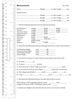
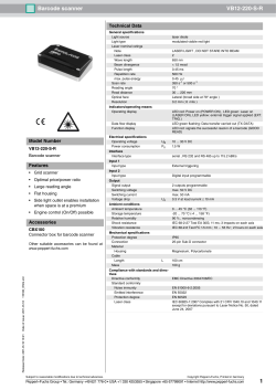
Metalization Pullback .005” typical
.0005” is possible for special requirements
ION BEAM MILLING, INC.
Laser Machined Features +/- .001”
THE BENEFITS ARE CUT AND DRY™
850 E. Industrial Park Drive
Manchester, NH 03109
Ph: 603-644-2326 Fax: 603-647-6889
www.ionbeammilling.com
Annulus .001” Min.
For Plated Through Vias
.002” Min.
Line/Gap Width
.0004” Min.
Tol. +/- .0001”
Typical Radius .006”
Typical Width .020”
.004” +/- .002”
Intrusion
1:1 Aspect Ratio
(Thickness to Diameter)
for Plated Wall Vias
Laser Cutout
Hole Location
+/- .001”
(Non-Cumulative)
0.006 min.
radius
Hole Diameter:
Thru Diameter +/- .002”
Surface Diameter +/- .001”
Metalization
Pullback .002”
Resistive Layer
Conductive Layer
Via to Artwork
Registration
+/- .001”
Passivated: Tantalum
Pentoxide for TaN, NiCR
may be Poliymide
Min. Via Hole
Separation
.025”
Copyright, 2009 Ion Beam Milling, Inc.
Laser Trimmed Layout
at 80% of Normal Value
Layer to Layer
Registration
+/-.0002”
Resistor Width
.001” Min.
Front to Back
Registration +/- .002
Maximum
outside
dimensions
of 4 inches
square
Diamond Blade Diced
+/- .001 L& W Standard
Length
.001” Min.
TaN Resistors
25-200 Ω/Sq.
No Overlap on
Conductor Pattern
© Copyright 2026 Paperzz