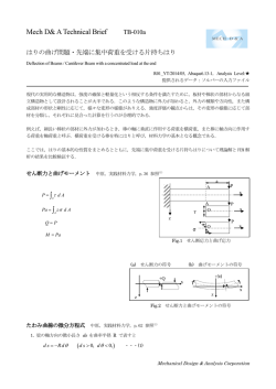
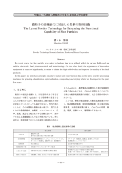
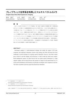
成 果 集
本成果集は,SPring-8 成果審査委員会において公開技術報告書の認定を受けております.
– 19 –
兵庫県ビームライン年報・成果集
BL08B2
2012B3302
BL08B2 における空間分解 XAFS 整備現状
Recent Developments of Spatially Resolved XAFS at BL08B2
李 雷 1 ,漆原 良昌 1 ,野瀬 惣市 2 ,横山 和司 1 ,桑本 滋生 1 ,竹田 晋吾 2 ,松井 純爾 1
Lei Li1 , Yoshimasa Urushibara1 , Souici Nose2 , Kazushi Yokoyama1 , Shigeo Kuwamoto1 ,
Shingo Takeda2 , Junji Matsui1
1
1
兵庫県立大学放射光ナノテクセンター,2 スプリングエイトサービス株式会社
Synchrotron Radiation Nanotechnology Laboratory, University of Hyogo, 2 SPring-8 Service Co. Ltd.
概要: 材料開発のニーズに応じて,空間分解 XAFS システムとして BL08B2 においてポリキャピラリー光
学系を採用してマイクロ XAFS および CCD カメラを用いて 2D イメージング XAFS を整備した.ポリキャ
ピラリーにより X 線を 25 μm 以下のビームに集光し,数十 μm 範囲での EXAFS スペクトルが得られること
が示された.また,イメージング XAFS は比較的に広い視野の構造情報を数ミクロン空間分解能で測定でき
ることが確認した.
キーワード: ポリキャピラリー,マイクロ XAFS,イメージング XAFS
背景と研究目的
光学系および測定系の性能評価
各種蓄電池などのエネルギー分野における材料開発
ポリキャピラリー集光素子は,X-ray Optics 社の製
において,空間分解 XAFS による構造解析の必要性が
品を選択した.適用するエネルギーを 6 keV から 15
認識されている.微小領域の構造情報を得るために,
keV の範囲として,光学系の性能評価を行った.具体
X 線集光ビームを試料上の所望の位置に照射させるこ
的な評価方法として,200 μm 径の白金ワイヤを用い
とで XAFS 測定が行われる.同様に構造情報を高位
たナイフエッジスキャン法によるビームサイズ測定や,
置分解能で取得可能とする方法として,二次元検出器
通過率,焦点位置(ワーキングディスタンス)を確認
を使用したイメージング XAFS も有効である.
した.形成した集光ビームを用い,光子エネルギー走
X 線の集光にはミラーや,ゾーンプレートや,キャ
査における光軸の安定性評価も行った.また標準試料
ピラリーなどの集光素子を用いた方法がある.最近で
として銅メッシュを使用して得られた X 線透過率の
は K-B ミラーやゾーンプレートによる集光方法が主
に採用されているが,BL08B2 では,偏向電磁石を光
源として実用的なビーム強度も意識しつつ,集光光学
系の検討を行った.ESRF の BM26A [1] を参考とし
て,ポリキャピラリー集光素子を採用した.
イメージング XAFS の場合,比較的均一な断面強
度分布を持ったブロードビームをプローブとして用
いる.高位置分解能性能を有する二次元 X 線検出器
を試料後方に配して,透過 X 線の二次元強度分布を
取得することで実現される.二次元 X 線検出器とし
て,BL08B2 では CCD カメラ素子とビームモニタと
を組み合わせたタイプのものを採用した.Fig. 1 に,
BL08B2 で整備した測定システム部分を示す.
– 21 –
Fig. 1. 2D imaging XAFS measurement system.
Status Report of Hyogo-Beamlines with Research Results, Vol. 2 (2013)
Table 1. Characteristics of Polycapillary Focusing Optics
Useful X-ray Energy Range
6∼10 keV
Size
8 mm, 50 mm
Working Distance
5 mm
Focused Beam Size
FWMH 25 μm ≥(6 keV)
Up to 25%(6∼10 keV)
Transmission Efficiency
測定データを検討し,EXAFS データ補正の妥当性も
した光学系での測定結果である.両方の光学系で測定
検証した.
された結果には,大きな違いは無かった.
イメージング XAFS 測定系の評価用試料として,銅
以上により,ポリキャピラリー集光素子による銅の
メッシュを使用した(ピッチ 42 μm,線幅 5 μm).ま
位置分解 XAFS が可能であることを実証できた.現
た,マンガンの価数が異なる,MnO と LiMnO2 の微
在は,その他の光子エネルギー領域における実証実験
粒子を混合した試料も準備した.二次元 X 線検出器
や,蛍光 XAFS や Quick XAFS への応用,化学状態
のビームモニタ部分に採用した蛍光体としては,P43
マッピング測定などの実用性の検証を行っている段階
(Gd2 O2 S: Tb) と YAG(Y3 Al5 O12 )であり,それぞ
である. れについて EXAFS 測定に適用し比較検討した.
イメージング XAFS は XANES 領域に限ると,蛍
光体 P43 が YAG に比べて,可視光変換効率の点で有
結果および考察
利であり,迅速な測定が可能であることを実験により
ポリキャピラリー集光素子の製品仕様を Table 1 に
示す.仕様範囲の光子エネルギーを超えて,15 keV に
おいても評価を行っている.光子エネルギー 6 keV の
評価結果では,集光点における鉛直方向におけるビー
ムサイズとしては,半値幅として 20 μm であること
を確認した.水平方向については,23 μm であった.
通過率も 40%以上あることを確認した.
Fig. 2 は集光光学系の性能評価の結果である.また
銅の K 吸収端近傍における光子エネルギー範囲にお
確認した.蛍光体が YAG の場合,1素子あたりの感
度の点では実用性が乏しいものの,20 ピクセル ×20
ピクセルの範囲を指定した binning 処理を施すことに
より,EXAFS 領域におよぶ実用的な測定が可能であ
ることを確認した.ここで,CCD 素子のピクセルサ
イズとしては,1 素子あたり 1.73 μm × 1.73 μm であ
る.Fig. 3 は MnO と LiMnO2 混合物の測定結果で
ある.Fig. 3a は,各酸化物単体で測定した XANES
スペクトルを重ねて表示したものである.このスペク
トル上で,混合試料の場合の光子エネルギー条件を決
いて EXAFS 測定を行った結果も示している.
光軸の安定性とポリキャピラリー集光素子の通過率
定した.
Fig. 3b は,K 吸収端位置が示すエネルギーよりも
を評価した実験結果を,それぞれ Fig. 2a および Fig.
2b に示す.光軸の重心位置は,光子エネルギー走査の
間,大きな位置のドリフトは生じなかった.ビームが
有する半値幅と比べても,僅かなドリフト量である.
高い 6.565 keV 条件に固定して取得した,透過 X 線
強度のイメージング像である.二次元 X 線検出器に
おいて使用した蛍光体は YAG である.
同じ検出システムを用い,別のエネルギー条件で取
集光素子が示す通過率については,光子エネルギー範
囲において大きな変化は確認さなかった.以上の結果
より,銅の K 吸収端近傍において,実用的な位置分
得した結果を Fig. 3c および 3d に示す.入射 X 線の
二次元強度分布については試料を光軸上より退避させ
ることで取得し,これを吸収度の二次元分布計算に使
解 XAFS が可能であることが確認できた.
銅箔を用いた EXAFS 測定結果および振動抽出した
結果を Fig. 2c および Fig. 2d に示す.EXAFS スペ
クトルは,バックグラウンド処理を施していないもの
用した.なお吸収量が高くなる領域での統計精度を高
めるために,20 ピクセル ×20 ピクセル範囲の binning
処理を施している.
Fig. 3c は,MnO の K 吸収端よりも高く,LiMnO2
を示している.黒線が通常の XAFS 測定光学系を用
いた場合であり,赤線がキャピラリー集光素子を使用
の K 吸収端の位置立ち上がり位置にあたる光子エネ
– 22 –
兵庫県ビームライン年報・成果集
Fig. 3. a) K edge XANES spectrum.of MnO and
LiMnO2 , b) X-ray CCD images of the sample at
Fig. 2. a) Vertical knife-edge scans for incident Xray energy from 9 keV to 10 keV, b) Transmission
efficiency of the polycapillary as a function of X-
X-ray energy of 6.565 keV, c) Mapping of the normalized absorption coefficient at X-ray energy 6.555
keV, d) Mapping of the normalized absorption coefficient at X-ray energy 6.560 keV
ray energy for the energy range scanned for the Cu
foil, c), d) Transmission XAFS spectra for Cu foil
recorded with and without polycapillary
– 23 –
Status Report of Hyogo-Beamlines with Research Results, Vol. 2 (2013)
ルギー条件に固定して撮像した透過 X 線のイメージ
今後の課題
像である.光子エネルギーは 6.555 keV である.Fig.
3d は,MnO および LiMnO2 の両方の K 吸収端より
も高いエネルギー位置で撮像した結果である.光子エ
ネルギーは 6.560 keV である.化学状態の異なる2種
類の酸化マンガンを混合した場合において,K 吸収端
付近での光子エネルギー条件の僅かな違いを,コント
ラストの二次元分布の違いとして鮮明に捉えることが
できた.同様にして異なる光子エネルギー条件でデー
タを取得し,相互の差分処理を施すことで,MnO と
LiMnO2 それぞれの状態分布を区別して二次元分布と
イメージング XAFS に関する,蛍光体種類および
測定条件を検討しながら,EXAFS の測定 S/N を改善
していく.また,今後は,産業界ユーザーのニーズに
応じて測定系の最適化を施し,性能実証を行った上で
供用する予定である.
参考文献
[1] G. Silversmit, B. Vekemans, S. Nikitenko, W.
Bras, V. Czhech, G. Zaray, I. Szaloki, and L.
Vincze, J. Synchrotron Rad. 16, 237-246 (2009).
して捉えることが可能であると考えられる.
– 24 –
兵庫県ビームライン年報・成果集
BL08B2
2013A3326
有機薄膜材料の X 線散乱構造解析
Structural Analysis of Organic Thin Films by X-ray Scattering
鈴木 拓也,岡部 崇志,小島 優子 ∗
Takuya Suzuki, Takashi Okabe1, Yuko Kojima∗
三菱化学科学技術研究センター
Mitsubishi Chemical Group Science and Technology Research Center, Inc.
概要: リオトロピッククロモニック液晶を示す材料として知られる sunset yellow FCF (the disodium salt 6-hydroxy-5-[(4-sulfophenyl)azo]-2-naphthalenesulfonic acid) における,せん断誘起による分子配向および構
造形成過程の機構に着目し,塗布によるせん断後の水の蒸発に伴う分子の配向と凝集過程を,時分割 GI-WAXS
により評価した.
キーワード: chromonic, liquid crystals, aggregation
背景と研究目的
実験
イオン基を有する分子の自発的な高次構造形成によ
試料
り実現されるリオトロピッククロモニック液晶 (LCLC)
は,広く研究されてはいるものの構造形成機構そのも
sunset yellow FCF 水溶液(濃度;31 wt%)
装置
のがよく理解されていないソフトマターの分類に位
BL08B2
置づけられる [1].水中では,LCLC 分子は互いに面
測定条件
同士が向かい合い水との界面にイオン基を配置したス
・波長;1.0 ˚
A タック型の凝集構造(H-aggregation)を形成するこ
とが知られている.しかしながら,凝集構造の形成機
構,分子の濃度や温度,イオン強度の影響といった,
LCLC の構造形成に関する根本的なメカニズムは,未
だ未解明な部分が多い.
・カメラ長;158.7 mm
・検出器;PILATUS
・入射角;0.20◦
・露光時間;2.5 秒 (インターバル;3.0 秒)
我々は,LCLC 材料としてよく知られる sunset yel-
自動塗布機を用いて試料液を塗布し,塗布方向と垂
low FCF (SSY)(the disodium salt 6-hydroxy-5-[(4-
直方向にX線を照射した.塗布直後から 1 測定時間
sulfophenyl)azo]-2-naphthalenesulfonic acid) におけ
3.0 秒での連続測定を行った.
る,せん断誘起による分子配向および構造形成過程の
機構に着目した.SSY 分子の構造をナノオーダーで定
結果および考察
量的に評価する有力な手法が X 線散乱/回折法であ
り,これまでに,H-aggregation 構造やスタックした
分子間における相互作用の評価に関する研究例などが
報告されている [1, 2].本研究では,BL08B2 を用い,
Fig. 1 に,(a) in-plane,(b) out-of-plane の 3D プ
ロファイルを示す.塗布直後は明瞭なピークが見られ
ず,SSY 分子は比較的ランダムに分散していると推定
塗布によるせん断後の水の蒸発に伴う SSY 分子の配
される.時間とともに,in-plane では2つのピーク,
向と凝集過程を,時分割 GI-WAXS により評価した.
out-of-plane では1つのシャープなピークが現れた.
これは,水の蒸発とともに,SSY 分子の面と平行およ
び垂直方向における凝集構造の形成が進展したことを
∗ 三菱化学科学技術研究センター分析物性センター
Mitsubishi Chemical Group Science and Technology Research Center, Inc. Materials Analysis Center
示している.
– 25 –
Status Report of Hyogo-Beamlines with Research Results, Vol. 2 (2013)
Fig. 1. 3D GI-WAXS results of (a) in-plane,(b) out-of-plane profiles.
Fig. 2. 2D GI-WAXS results of (a) in-plane,(b) out-of-plane profiles.
Fig. 2 に,(a) in-plane,(b) out-of-plane の 2D プ
ロファイルを示す.in-plane に関して,広角側のピー
˚ に対応しており,SSY 分子の π 相互作
クは d=3.4 A
用による面同士のスタックを反映している.低角側の
ピークは d=12.6 ˚
A に対応する長周期構造の形成を示
今後の課題
今回,SSY 分子のせん断誘起による配向および溶媒
の蒸発に伴う構造形成過程の機構を時分割 GI-WAXS
を用いて推定できた.今後は,せん断速度の影響や濃
唆している.Out-of-plane に関して,最終的に d=18.7
˚
A に対応するピークが観測された.これは,SSY 分
子のイオン基同士の静電反発による周期構造と推定さ
れる.また時間と共に広角シフトしており,水の蒸発
による周期サイズが減少したと考えられる.
Fig. 3 に,色素の面同士のスタックに対応するピー
クの方位角プロファイルを示す.φ=0◦ が赤道方向で
ある.赤道方向の強度は,塗布直後はやや高く,時間
とともに増大しているのがわかる.これは,塗布直後
はせん断による配向がわずかに生じており,水の蒸発
に伴い配向が顕著に進展したことを示している.
Fig. 3. 2D azimuthal angle profiles evaluated from
the face-to-face aggregation peak.
– 26 –
兵庫県ビームライン年報・成果集
度・温度に着目し,LCLC の構造形成に関するメカニ
参考文献
ズムの詳細を把握することが課題と考える.
[1] H-S. Park et al., J. Phys. Chem. B 112 1630716319 (2008).
[2] J. Lydon, Liquid Crystals 38, 1663-1681 (2011).
事業への貢献
本研究で得られた成果は,LCLC 材料の薄膜中にお
けるせん断誘起の構造形成機構を示したことであり,
新規な LCLC 材料の設計指針を提示するという意味
で事業に貢献した.
– 27 –
Status Report of Hyogo-Beamlines with Research Results, Vol. 2 (2013)
BL24XU
2011B3247, 2012A3247, 2012B3247
4 次元 X 線 CT を用いたポリマーフォームの気泡形成挙動観察
Cell Growth Observation of Polymer Foam by 4D X-Ray CT
中野 真也
Shinya Nakano
日東電工株式会社 機能設計技術センター
Functional Design Technology Center, Nitto Denko Corporation
概要: 熱をトリガとして発泡することで気泡構造を形成するポリマーフォームにおいて,気泡が生成・成長・
合一するメカニズムについてはよく知られてない.本検討では 4 次元 X 線 CT を用いて,加熱によるポリマー
フォームの気泡形成過程を動的観察した.その結果,昇温速度によって発泡開始温度や気泡径が変化すること
が示された.これにより,気泡の構造を任意に制御した発泡体を設計できる可能性が示唆された.
キーワード: X 線 CT,ポリマーフォーム,加熱発泡,気泡構造制御
背景と研究目的
かった範囲での製品設計が求められており,より高度
自動車に使用される部材として,水・音・振動など
を防止する目的で,種々のポリマーフォーム材料が用
いられている.これら材料の多くは熱をトリガとし
な設計指針の獲得が望まれる.そこで本検討では,4
次元 CT を利用してポリマーの加熱発泡挙動を動的に
観察することにより,発泡メカニズムの解明を目指し
て化学的に発泡し,多孔質構造を形成する.ポリマー
ている.ここでは,昇温速度による気泡形成挙動の違
フォームの構造パラメータは要求される機能に応じて
いについて比較した結果を報告する.
設計されることが望ましいが,現状では気泡が生成・
成長・合一するメカニズムは明確になっておらず,経
実験
験的な指標に依存する部分が多い.今後の製品展開と
しては,例えば気泡の微細化など従来制御できていな
観察対象としてゴム系発泡体材料を選択し,実験で
は発泡前の樹脂混和物を試料に用いた.樹脂混和物
Fig. 1. Schematic illustration of the X-ray CT observation system.
– 28 –
兵庫県ビームライン年報・成果集
は縦 1.2 mm,横 1.7 mm であることから,発泡によ
る膨張を考慮して 0.5 mm 角程度の大きさに試料を
切り出して回転ステージに設置した.試料を透過し
たビームを CWO 蛍光体で可視光に変換し,リレー
レンズで高速度 CMOS イメージセンサ(フォトロン
FASTCAM SA5)に導入した.このときの観察分解
能は 2 μm/pixel であった.試料を設置したステージ
をグラファイトのカバーで覆い,外部よりハロゲンラ
ンプヒーターで加熱した.放射温度計を用いてグラ
ファイトカバーの外表面温度を測定し,フィードバッ
ク制御によりハロゲンランプヒーターの出力を制御
し,昇温速度を調節した.昇温速度は 2◦ C/min およ
び 5◦ C/min とした.なお内部と外表面とでは温度差
があることから,あらかじめ熱電対を用いて温度検量
線を作成し,外表面温度からの換算値を内部温度とし
て用いた.
試料を 0.1 rps で回転させ,放射光 X 線ビームを
照射しながら所定の昇温速度となるように加熱を行っ
た.撮影速度は 125 fps(露光時間 8 ms)であるが,
今回の系では比較的低速で発泡が進行するため,昇温
速度に応じて数十秒間隔ごとに CT 構成に必要な投影
Fig. 2. CT image of foam forming behavior, (a) normal stereoimage and (b) extracted cells by image
processing.
像(本条件では半回転あたり 625 枚)を取得した.得
られた投影像から 3 次元再構成計算を行い,CT 像を
得た.さらに CT 像に対して二値化処理を行い,内部
気泡の直径を定量的に解析した.
結果および考察
Fig. 2 に,再構成像および二値化により抽出した
気泡の例を示す.これらの画像により経時すなわち昇
温による気泡成長や,それに伴う合一・破裂などの動
的挙動を初めて可視化することができた.また生成後
間もない数 μm の微小な気泡を観察出来ることから,
高い空間分解能が得られたと言える.Fig. 3 に二値化
像から求めた平均気泡径の,温度上昇に伴う推移を示
す.2 ◦ C/min に比べて 5 ◦ C/min では気泡が生成を
Fig. 3. Average cell diameter trend with rising temperature.
始める温度が高く,また気泡が大きく成長することが
わかる.このように,昇温速度によって気泡の直径を
制御できる可能性が示唆された.気泡は,まず発泡剤
には発泡剤が配合されており,加熱によって分解し,
発生するガスによって気泡を生成する.BL24XU の
B ブランチ [1] に構築した実験系の概要を Fig. 1 に
示す.放射光 X 線ビーム(10 keV)による最大視野
が熱分解してガスが発生し,次に周囲の樹脂が膨張す
ることで生成・成長する.このことから,昇温速度の
違いが発泡剤の分解と樹脂の膨張それぞれにどのよう
に影響を及ぼすのかを精査することが,今後の製品設
計のために重要と考えられる.
– 29 –
Status Report of Hyogo-Beamlines with Research Results, Vol. 2 (2013)
今後の課題
かったポリマーフォームの加熱発泡挙動に対して,基
発泡剤や樹脂の物性を評価し,発泡挙動と比較考察
していく.また異なる材料系の発泡挙動観察も併せて,
発泡を精密に制御出来る理論の構築を目指す.
事業への貢献
礎的かつ重要な知見を与えるものであり,今後の弊社
事業に対して多大な貢献をもたらすことが期待される.
参考文献
[1] 高野秀和:兵庫県ビームライン年報・成果集 1,
61-66 (2012).
本研究で得られた成果は,従来よく知られていな
– 30 –
兵庫県ビームライン年報・成果集
BL08B2, BL24XU
2012A3229, 2012B3229, 2012B3330
小角 X 線散乱法と逆モンテカルロ法を用いた構造発色フィルムの構造解析
Small Angle X-ray Scattering and Reverse Monte Carlo Analysis
of Colloidal Silica Arrays in Cross-Linked Polyacrylate Films
首藤 靖幸 1 ,妹尾 政宣 1 ,横山 和司 2 ,李 雷 2 ,桑本 滋生 2 ,漆原 良昌 2 ,竹田 晋吾 2 ,
中前 勝彦 2 ,松井 純爾 2
Yasuyuki Shudo1 , Kazunobu Senoo1 , Kazushi Yokoyama2 , Lei Li2 , Shigeo Kuwamoto2 ,
Yoshimasa Urushihara2 , Shingo Takeda2 , Katsuhiko Nakamae2 , Junji Matsui2
1
住友ベークライト株式会社,
1
2
2
兵庫県立大学放射光ナノテクセンター
Sumitomo Bakelite Co., Ltd.,
Synchrotron Radiation Nanotechnology Laboratory, University of Hyogo
概要: ナノシリカ粒子を充填した構造発色透明複合基板の構造と光学特性の関係を解明するため,複合フィ
ルムの小角 X 線散乱 (SAXS) 測定と逆モンテカルロ法 (RMC) による三次元的な粒子分散状態の解析を検討
した.RMC により得られたナノ粒子の動径分布関数を解析した結果,粒子充填量の増加に伴い粒子間の短距
離秩序が形成されていることが示唆される結果を得た.また動径分布関数の第一ピーク位置から算出した粒子
間距離は FE-SEM の観察結果と概ね一致した.
キーワード: 小角 X 線散乱,極小角 X 線散乱,Bonse-Hart USAXS,構造発色,ナノコンポジット,逆モ
ンテカルロ法
背景と研究目的
ニックバンドギャップ形成の要因となりうることが明
我々は架橋ポリマーネットワーク中にナノシリカ粒
子を充填させることによって,高耐熱性と低線膨張率
係数を両立する透明プラスチック複合フィルムを開発
した [1–3].更に,我々は特定の粒子径および粒子充填
量において,色素等を含有していないにも関わらず可
視光の特定波長のみを反射するような発色性フィルム
を得た.この発色現象は構造発色として知られ,コロ
イド粒子の結晶配列による光の回折反射は構造発色の
代表例である [4].これまでの検討で,我々は複合フィ
ルム中のナノ粒子の分散状態の解析には SPring-8 に
おける高輝度放射光を利用した小角 X 線散乱 (SAXS)
測定および構造因子解析が有効であることを確認した.
しかしながら 3 次元パラクリスタル理論 [5] を用いて
SAXS プロファイルの解析をおこなった結果,我々の
開発した材料はコロイド結晶型の長距離秩序構造は
形成していないことが示唆された.近年の研究では,
らかになり [6],我々の材料においても光学特性の発
現には幾つかの機構が複雑に絡みあっているものと考
えられる.したがって光学特性発現機構を解明しその
特性を制御するためには材料の三次元構造を明らかに
することが必要である.
ナノフィラー分散系における三次元的なフィラー配
置の推定手法として,逆モンテカルロ法 (RMC) は有
効な手法の一つである [7].本来,RMC は無機系材料
の不規則構造解析手法として開発されたが,近年では
ナノフィラー系へも適用範囲が拡大されている [8].本
研究ではナノシリカ粒子を架橋ポリマーネットワーク
中に固定させて得た複合フィルムにおける粒子分散状
態と構造発色性の関係を解明するため,SAXS と RMC
を用いた粒子の三次元分散状態の解析を検討した.
実験
コロイド粒子の短距離秩序構造やコロイド粒子自身の
本検討で使用した試料は次に記載する方法で作成
Mie 散乱なども構造発色,つまり可視光領域のフォト
した.まず,二官能アクリレートモノマー,イソプ
– 31 –
Status Report of Hyogo-Beamlines with Research Results, Vol. 2 (2013)
ロパノール分散型コロイダルシリカ(平均粒子径約
120 nm)および光重合開始剤を配合し,溶媒を減圧
下にて除去した.その後,シート成形し積算光量約 700
mJ/cm2 の紫外光により架橋し,さらに 230◦ C で 3 時
間アニール処理することにより,膜厚約 200 μm のフィ
ルムを得た.シリカの体積分率 η は η = 0.001–0.50
とし,種々の充填量のサンプルを調整した.
SAXS 実験は兵庫県ビームライン BL08B2 の第 2 ハ
ッチにて実施した.検出器には 2 次元検出器 PILATUS
を用い,カメラ長および波長は 6.2 m, 1.5 ˚
A と 1.6 m,
1.0 ˚
A の 2 条件でおこなった.USAXS 実験は兵庫県
ビームライン BL24XU の A1 実験ハッチにて実施し
た.Bonse-Hart 光学系と 1 次元シンチレーション検
出器を用い,10 keV のエネルギーの X 線を利用し測
定した.
RMC シミュレーションは RMC++ (ver.1.6.1) [9]
を用い, FOCUS スパコン A システム(財団法人 計算
科学振興財団)にて実施した.計算条件等の詳細は以
下に述べる.
Fig. 1. SAXS and USAXS profiles of composite
films containing various volume fractions η of silica particles.
として扱った.シリカ粒子の数密度 ρ は,粒子の体積
分率 η と粒子の平均体積 v から
結果および考察
η = ρv
SAXS および USAXS 実験より得られた連結後の一
次元プロファイルを Fig. 1 に示す.いずれのサンプル
についても SAXS の二次元散乱プロファイルは等方
的であり,配向性や強い結晶的秩序性を有していない
ことから,Bonse-Hart USAXS の一次元プロファイ
ルとの連結には問題ないものと考えた.フィルム中に
含まれるシリカ粒子の平均粒径およびその粒度分布は
以前に検討した手法 [3] により η = 0.001 のサンプル
の SAXS プロファイルから算出した.得られた平均
粒子半径 R0 は 60 nm,CV 値 (= σ/R0 ) は 6.3 %と
ほぼ単分散とみなせることがわかった.また,各充填
量における構造因子 S(q) は η = 0.001 のサンプルの
によって得た値を用いた.ここで,平均体積 v は
∞
4 3
v=
πR p(R)dR
3
0
である.粒子半径 R の分布関数 p(R) は Gauss 分布
を仮定し,平均粒子半径 R0 と標準偏差 σ は前述の
SAXS プロファイルに関するフィッティング結果を用
いた.RMC においては粒子同士の重なりを防ぐため
にカットオフ距離 rcut を設定することができ,本検
討では rcut= 2R0 とした.また,系中の全粒子数は
4000,初期配置は FCC 構造とした.
Fig. 2 に補正後の構造因子 S(q) と RMC による
SAXS プロファイルで除し規格化することによって導
フィッティングの結果を示す.いずれの充填量 η にお
出した.
RMC シミュレーションは以下の順で実施した.まず,
上記手続きにより得られた構造因子について MCGR
[10] を用いてバックグラウンド,規格化定数等の補正
をおこない,得られた構造因子プロファイルを RMC
の入力として供した.RMC においてはナノ粒子を単
いても,入力に用いた S(q) をほぼ再現する三次元構
造が得られた.η = 0.33, 0.40 の高充填量では極小角
領域においてフィッティングが悪くなっているが,こ
れは系のシステムサイズの不足に由来する問題であり,
粒子数を大きくすることで改善可能と考えられる.
Fig. 3 に各構造に対応する粒子間の動径分布関数
位粒子として直接扱うことはできないため,系全体の
スケールを 1/1000 に縮小し,シリカ粒子を擬似原子
g(r) を示す.η > 0.20 においては動径分布関数に鋭い
第一ピークが現れているが,η < 0.20 では第一ピーク
– 32 –
兵庫県ビームライン年報・成果集
Fig. 3. Pair distribution function g(r) of silica
particles for various volume fractions η obtained
from RMC simulation.
Fig. 2. Structure factor S(q) for individual samples obtained from SAXS and USAXS experiments after refinement using MCGR and their fitting results by RMC simulation.
はブロード化しており,粒子充填量 η の増加に伴って
短距離秩序構造が形成されていることがわかる.また,
いずれもカットオフ距離近傍で小さなピークが現れて
いるが,これは実験値とのパラメータの誤差や RMC
のアルゴリズムに由来するノイズと思われる.
Fig. 4 に g(r) の第一ピーク位置から求めた最近接
粒子間距離と,フィルム表面の FE-SEM 観察結果か
ら算出した最近接粒子間の関係を示す.両者の値は概
ね一致していることから,RMC シミュレーションの
結果がある程度妥当なものであることが示唆される.
低充填量においては値の乖離が大きいが,これは粒子
位置および粒子間距離のばらつきが大きいことによる
ものと考えられ,詳細な比較評価には Voronoi 領域解
Fig. 4. Distance between particles from RMC simulation and calculated from FE-SEM images on
sample surfaces.
析などを検討する必要があると思われる.
ある.光学特性と構造の相関解明には,数値解析等に
今後の課題
よる三次元構造の秩序性評価や FDTD 法などによる
本研究では SAXS および RMC によるナノシリカ
粒子の三次元分散状態の解析を検討した.今後の課題
としてはシミュレーションの妥当性検証,高精度化お
よび光学特性との相関解明手法の検討が挙げられる.
シミュレーションの高精度化には,形状因子と構造因
子の分離方法の再検討,RMC のパラメータの十分な
吟味をおこなう必要がある.また,USAXS 測定結果
電磁界シミュレーションが有効と考えられる.
今後は極小角領域の構造の追検証や実空間像の観察
等も実施し,X 線構造解析と実空間構造解析,各種シ
ミュレーションを交えた構造と光学特性の相関解明を
おこなっていく.
事業への貢献
を十分に反映させるためには今回検討した粒子数では
本研究で得られた成果は,住友ベークライト株式会
不足であり,セルサイズを数 μm 立方,粒子数を十万
社における透明ナノコンポジットフィルム開発におい
程度とする大規模シミュレーションを実施する必要が
– 33 –
Status Report of Hyogo-Beamlines with Research Results, Vol. 2 (2013)
て,材料中の構造形成および制御に関する要素技術の
構築に貢献があった.
参考文献
[1] K. Senoo, T. Takeuchi, W. Oka, Y. Shimobe,
S. Kuwamoto, Y. Urushihara, J. Matsui, and
K. Nakamae, J. Network Polym., Jpn. 30, 16
(2009).
[2] K. Senoo, T. Takeuchi, W. Oka, Y. Shimobe,
S. Kuwamoto, Y. Urushihara, J. Matsui, and
K. Nakamae, J. Network Polym., Jpn. 31, 19
(2010).
[3] Y. Shudo, M. Miyake, K. Sato, K. Senoo, S.
Kuwamoto, 兵庫県ビームライン年報・成果集 Vol.
1, 44 (2011).
[4] S.-H. Kim, S. Y. Lee, S.-M. Yang, G.-R. Yi,
NPG Asia Mater. 3, 25 (2011).
[5] H. Matsuoka, H. Tanaka, T. Hashimoto, and N.
Ise, Phys. Rev. B 36, 1754 (1987).
[6] S. F. Liew, J.-K. Yang, H. Noh, C. F. Schreck,
E. R. Dufresne, C. S. O’Hern, H. Cao, Phys.
Rev. A 84, 063818 (2011).
[7] R. L. McGreevy, L. Pusztai, Mol. Simul. 1, 359
(1988).
[8] K. Hagita, T. Arai, H. Kishimoto, N. Umesaki,
Y. Shinohara, and Y. Amemiya, J. Phys. Condens. Matter 19, 330017 (2007).
[9] http://www.szfki.hu/ nphys/rmc++/opening.
htm
[10] L. Pusztai, and R. L. McGreevy, Physica B
234-236, 357 (1997).
– 34 –
兵庫県ビームライン年報・成果集
BL24XU
2010B3200, 2011A3200, 2011B3200
Inclined-incidence Microprism-array Optical Device
for Prefocusing Hard X-ray Beams
Y. Kagoshima1 , H. Takano1 and S. Takeda2
1
Center for Novel Material Science under Multi-Extreme Conditions,
Graduate School of Material Science, University of Hyogo,
2
SPring-8 Service Co., Ltd.
Abstract: A microprism-array optical device has been developed that can roughly focus a hard Xray beam to increase the photon flux density at the sample position. As it operates in a transmission
arrangement that produces negligible beam deflection, the need for additional equipment is minimal
when it is introduced in existing facilities. The effective apex angles of the microprisms can be changed
by varying the inclination angle; this allows the focal point to be easily changed. A prototype device is
fabricated from a 300-μm-thick acrylic resin plate. It consists of 20 50-μm-wide right-angle microprisms
whose apex angles gradually decrease to 22.2◦ at the outer side. The effective apex angle can be reduced
to 3.6◦ at an inclination angle of 80.5◦ . Its focusing performance was numerically evaluated by ray tracing
that accounted for absorption. The results predict a gain in the photon flux density of ∼25 for a crossed
tandem arrangement. In experiments using an X-ray energy of 10 keV, a 680 μm (V) × 660 μm (H)
beam was focused to a spot size of 130 μm (V) × 380 μm (H), resulting in a photon flux density gain of
∼3. The present microprism-array optical device can be used to improve beamlines for experiments that
do not require microfocusing such as X-ray absorption fine structure spectroscopy, powder diffraction,
and small-angle scattering experiments.
本報告書は原著論文(Y. Kagoshima et al., J. Appl. Phys. 113, 214314 (2013).)を拡充・改編したもので
ある.
Keywords: X-ray refraction, X-ray microprism, X-ray focusing, prefocusing, microprism array
reflection mirrors is expensive since they require a
Introduction
Grazing-incidence total-reflection mirrors are
widely used as optical prefocusing devices in
many beamlines at synchrotron radiation facilities
throughout the world to increase the photon flux
density of beams irradiated onto samples. However,
if a total-reflection mirror is added to an existing
beamline to increase the photon flux density, the reflected beam is intrinsically deflected, necessitating
a major reconstruction of the beamline. If a twomirror system is used to ensure that the reflected
beam remains parallel to the original beam, the
beam will be offset. Furthermore, introducing total-
vacuum chamber and a precision alignment system.
Therefore, an optical device that operates in a transmission arrangement is preferable for increasing the
photon flux density of existing beamlines with as little reconstruction as possible. One solution, which
was first experimentally demonstrated by Snigirev et
al. [1], is to use a compound refractive lens (CRL).
It has a relatively simple operation principle and is
useful for beam focusing. Lengeler et al. [2] and
Schroer et al. [3] extended the concept by employing parabolic-shaped microlenses. Although CRLs
are effective as a nano- and microfocusing lenses,
– 35 –
Status Report of Hyogo-Beamlines with Research Results, Vol. 2 (2013)
they are not particularly suitable as optical prefocusing devices for beamlines because they have small
apertures and non-negligible absorption (especially
in their outer regions). Other refractive X-ray lenses
have been developed. Ohishi et al. [4] developed a
refractive X-ray lens consisting of many plastic lens
chips fabricated by molding as an optical prefocusing
device for beamlines for high-pressure X-ray diffraction experiments. Kohmura et al. [5] used a thin
glass microcapillary filled with an adhesive or glycerol containing bubbles. Since it employs the same
operation principle as a CRL, it has a non-negligible
absorption in the outer regions. Another solution
is to use a Fresnel zone plate. Fresnel zone plates
have been used as microscope objectives with a spatial resolution of almost 10 nm (Chao et al. [6] and
particularly suitable as beamline prefocusing devices
Fig. 1. Illustration of microprism array. (a) Onedimensional focusing by a single array and (b)
crossed tandem arrangement for two-dimensional fo-
because they have intrinsically low diffraction effi-
cusing.
Vila-Comamala et al. [7]). However, they are not
ciencies.
In this paper, we propose a simple refractive optical prefocusing device to enhance existing synchrotron radiation beamlines. It consists of an array
of right-angle microprisms whose apex angles gradually decrease toward the outer side. Since it operates
in a transmission arrangement with negligible beam
deflection, minimal additional equipment is required
when it is introduced into existing facilities. The
present device is effective for beamlines that do not
require microfocusing such as X-ray absorption fine
structure, powder diffraction and small-angle scat-
be greatly reduced from that for normal incidence
(see Fig. 1(a)). Furthermore, by arranging two microprism arrays in a crossed tandem arrangement,
two-dimensional focusing can be achieved (see Fig.
1(b)). An incident X-ray beam is refracted twice
when it passes through a right-angle microprism (see
Fig. 2). The microprism is assumed to be inclined
at an angle of θ relative to the incident beam. The
complex refraction index, n, of the microprism material is expressed by n = 1 − δ + iβ and that of air
is assumed to be unity. The prism has dimensions of
tering experiments.
w ×t× l and an apex angle of φa . The incident beam
Structure of Microprism Array and Optical
Design of Prototype
impinges on the microprism at P with an angle of incidence θ and is refracted with an angle of refraction
θ . The beam is refracted again at the microprism
1) Operation principle
surface at Q with an angle of incidence σin and exits
The microprism array employs a very simple focus-
the microprism with an angle of refraction σout . All
ing principle that is depicted in Fig. 1. Like visible
these processes obey Snell’s law:
light, X-ray refraction obeys Snell’s law. However,
since most materials have X-ray refraction indices of
almost unity, an X-ray beam will be deflected very
little by prisms with conventional apex angles. By
inclining a microprism, its effective apex angle can
– 36 –
sin θ = (1 − δ) sin θ
(1)
(1 − δ) sin σin = sin σout .
(2)
兵庫県ビームライン年報・成果集
Fig. 2. Optical path of incident ray in a single rightangle microprism.
the deflection angle at Q is α (i.e., the angle between
−→
−→
PQ and QR). Regarding refraction at Q, P, Q, and
R lie in the plane of incidence, which is denoted by
the rectangle abcd . A section of the microprism that
Fig. 3. Structure of prototype microprism array.
where r is the distance from the center of the microprism array O to the corresponding microprism
under the assumption that the microprism array is
much smaller than f .
contains the plane of incidence is denoted by the
2) Design and fabrication of prototype micro-
triangle ABC. By inclining the microprism, the ef-
prism array
fective apex angle can be reduced to φ. φ can be
To suppress absorption as much as possible, the mi-
geometrically derived to be
croprism array should be minimized. The micro
tan φa
, F (θ , φa ) =
tan φ =
F (θ , φa )
tan2 θ
1+
,
cos2 φa
prism array was fabricated by a company that pro(3)
duces custom-made optical Fresnel lenses. The microprism arrays were fabricated by sheet-press form-
where θ can be obtained from eq. (1). For normal
ing using acrylic resin sheets as the microprism ma-
incidence, θ is zero, and thus φ = φa . When used
terial. The minimum microprism size and the apex
as a prefocusing device, the absorption must also be
angle were limited by the precision of the transla-
considered. The average transmission < T > is given
tion stages and the sharpness of the tool bit used to
by
machine the metal mold. We employed a constant-
1 − exp(−μ l02 + t2 )
< T >=
,
μ l02 + t2
width microprism array for the prototype. The width
(4)
assuming that the incident beam is parallel to the
optical axis, where μ(= 4πβ/λ) is the linear absorption coefficient of the microprism material and l0 is
the effective microprism length, which is determined
by the angle of incidence θ. The focal length is assumed to be long since the microprism array is to be
used as a prefocusing device. The focal length f can
be approximated by
r
cos θ · F,
f∼
tan α
w was designed to be 50 μm and the minimum (outermost) apex angle φa was designed to be 22.2◦ based
on the present manufacturing limitations. Fig. 3
shows the designed structure of the microprism array. Table 1 lists the apex angles φa and the corresponding thicknesses t of the microprisms, which are
numbered 1 to 10 in Fig. 3.
The acrylic resin sheet was 300 μm thick. The
total width was 1 mm (= 20×50 μm), which was
designed to match the incident beam height of the
(5)
Hyogo ID-BL (BL24XU) beamline (Tsusaka et al.
[8]) of SPring-8. The total length l was designed
– 37 –
Status Report of Hyogo-Beamlines with Research Results, Vol. 2 (2013)
Table 1. Apex angles and thicknesses of prisms in
Fig. 3.
Prism
number
Apex angle: φa
(◦ )
Thickness: t
(μm)
1
2
3
82.66
68.89
57.22
6
19
32
4
5
48.01
40.81
45
58
6
7
8
35.23
30.85
27.39
71
84
97
9
10
24.58
22.22
109
122
Fig. 4. Scanning electron micrograph of fabricated
microprism array.
vertical angular beam divergences, respectively. The
to be 20 mm, which is long enough for a large in-
effective size Σx,y and angular divergence Σx ,y of
the photon beam are Σx,y = σx,y 2 + σp 2 and Σx ,y
= σx ,y 2 + σp 2 , respectively, where σp and σp are
clination angle. Fig. 4 shows a scanning electron
respectively the natural size and divergence of the
micrograph of the fabricated microprism array. It
photon beam. The natural size (divergence) is the
reveals that good microprism structures with com-
photon beam size (divergence) emitted from a single
paratively smooth surfaces were obtained, although
electron (or a zero-emittance electron beam). σp and
√
σp are expressed by σp = λL/4π and σp = λ/L,
the apexes are not perfectly sharp.
where λ is the photon wavelength and L is the toNumerical Evaluation of Focusing Performance
by Ray Tracing
tal length of the undulator (Kim [12]). Table 2 lists
the relevant electron beam parameters of BL24XU
and the effective photon beam parameters used in
1) Ray emission of undulator radiation
We employ three Cartesian axes to describe the synchrotron radiation optics [9]. The y-axis is taken to
be normal to the plane of the electron orbit and the
z-axis is taken to be tangential to the orbit. The
angles that a ray makes to the z-axis in the horizontal xz and vertical yz planes are denoted by x and
y , respectively. The x − x and y − y spaces are
termed horizontal and vertical phase spaces. The
Hyogo ID-BL (BL24XU) employs a figure-8 undula-
ray tracing. The photon energy E was set to 10
keV (λ=0.124 nm) and the total undulator length L
was taken to be 4.48 m (26 mm×172 periods). Figs.
5(a)-(d) show spot diagrams at the source points of
the x − y, x − y , x − x , and y − y , respectively. As
mentioned above, they all have Gaussian distributions with the standard deviations, Σx,y and Σx ,y ,
listed in Table 2. The number of emitted rays was
100,000.
tor developed by Tanaka and Kitamura [10]. The un-
2) Potential focusing ability of designed mi-
dulator radiation source has Gaussian distributions
croprism array
in the x − y, x − y , x − x , and y − y spaces. In this
The focusing properties of the prototype microprism
study, we used a ray emission algorithm developed
array were investigated by ray tracing. The complex
by Muramatsu et al. [11].
refraction index, n, of acrylic resin (C5 H8 O2 ) was ob-
In the following, σx and σy denote the standard de-
tained from the Center for X-ray Optics (Gullikson
viations of the horizontal and vertical electron beam
[13]) as δ = 2.67150153×10⁻⁶ and β = 3.71373554×
dimensions, respectively. Similarly, σx and σy de-
10−9 . First, only the vertical direction was assumed
note the standard deviations of the horizontal and
– 38 –
兵庫県ビームライン年報・成果集
Table 2. Relevant electron beam parameters for
BL24XU and effective photon beam parameters used in ray tracing.
Notation
Parameter
Unit
σx
σy
σ x
297.9
6.170
12.26
μm
μm
μrad
σy E
1.100
10
μrad
keV
σp
σp Σx
1.875
5.261
297.9
μm
μrad
μm
Σy
Σx 6.449
13.34
μm
μrad
Σy
5.375
μrad
to be focused (see Fig. 1(a)). The optical system
of BL24XU is shown in Fig.
6.
There are two
Fig. 5. Spot diagrams at the source point: (a) x − y,
(b)x − y , (c) x − x , and (d) y − y spaces.
pairs of experimental hutches: A1-A2 and B2-B1
(Takano [14]). The microprism array was located in
experimental hutch A1 and the incident beam was
focused in hutch A2. A four-quadrant front-end slit
(height: 1 mm; width: 1 mm) was located 30 m
from the source point and the microprism array was
located 46 m (z1 ) from the source point. The microprism array was inclined at an angle of 80.5◦ (θ1 )
Fig. 6. Optical system of BL24XU of SPring-8.
relative to the incident beam; its focal length f was
12 m according to eq. 5. Therefore, the beam will
be focused at a point 16.235 m (z2 ) from the microprism array according to the thin-lens formula,
1/z1 + 1/z2 = 1/f .
A double-crystal monochromator (monochromator A) with diamond crystals was employed for experimental hutches A1 and A2. Fig. 7 shows the
focusing properties for three different values of z2 .
Figs. 7(a), (c), and (e) show the real-space (x − y)
spot diagrams, while Figs. 7(b), (d), and (f) show
phase-space (y − y’) spot diagrams. Figs. 7(a) and
(b), Figs. 7(c) and (d), and Figs. 7(e) and (f) show
spot diagrams for z2 = 11.235 m (5 m upstream),
16.235 m (the focal point), and 21.235 m (5 m downstream), respectively. Figure 7 clearly confirms that
the beam is focused at z2 = 16.235 m, as predicted
by the thin-lens formula. The focused beam size
was ∼68 μm. In the phase-space spot diagrams,
each cluster corresponds to a refracted beam from
one microprism. Absorption was accounted for in
the ray tracing. The transmission (i.e., the ratio of
the number of transmitted rays to the number of incident rays) was 63.7%. As shown in Fig. 3, the
average absorption increased with increasing number of the microprisms. The average transmission
for all the microprisms was calculated to be 62.1%
using eq. 4. These two values for the transmission
are in good agreement with each other.
Next, both the vertical and horizontal directions
were assumed to be focused (see Fig. 1(b)). The
distance between the two microprism arrays was set
– 39 –
Status Report of Hyogo-Beamlines with Research Results, Vol. 2 (2013)
transmission was 63.7% in Fig. 8(b) and 39.7% in
Fig. 8(c). Here, we define the flux density in ray
tracing as the total number of rays divided by the
beam area (which is equal to the product of the vertical and horizontal FWHMs). Inserting perfectly
formed microprism arrays would increase the flux
density by factors of ∼7.3 in Fig. 8(b) and ∼25 in
Fig. 8(c). If the beam area is restricted to 50 μm×50
μm (red in Fig. 8), the flux density will be increased
by factors of ∼7.9 (Fig. 8(b)) and ∼23 (Fig. 8(c)).
Figs. 9(a)-(d) show the spot diagrams for a focused
beam in x − y, x − y , x − x’, and y − y spaces,
respectively. The beam patterns are upright in both
phase space directions (Figs. 9(c) and (d)), which
confirms that the beam is focused in both directions
at z2 = 16.235 m.
Feasibility Tests of Prototype Microprism Arrays
The focusing properties of prototype microprism
arrays were experimentally evaluated. A similar optical set to that shown in Fig. 6 was used. In hutch
A1, a four-quadrant slit (height: 1 mm; width: 1
mm) was placed 80 cm in front of the front microFig. 7. Spot diagrams of (a), (c), and (e) real space
prism array. Hutches A1 and A2 were connected by
(x − y) and (b), (d), and (f) vertical phase space
(y−y ) at z2 = (a) and (b) 11.235, (c) and (d) 16.235,
and (e) and (f) 21.235 m.
a 7.3-m-long vacuum path. To suppress air absorption, 4.3-m-long and 3.4-m-long vacuum paths were
aligned with the optical axes in hutches A1 and A2,
respectively. The air path was 1.3 m long and 53% of
to 0.2 m and the angle at which the second microprism array was inclined, θ2 , was set to 80.5◦ . Fig.
8 shows real-space spot diagrams at z2 = 16.235 m
(the focal point). Figs. 8(a), (b), and (c) respectively show real-space spot diagrams obtained with
no microprism arrays, with only the vertical microprism array, and with both prism arrays. The microprism arrays reduced the beam size (defined as
the full width at half maximum, FWHM) from 0.78
mm to 67 μm in the vertical direction and from 1.23
mm to 225 μm in the horizontal direction. The total number of rays was 50,856 in Fig. 8(a), 32,388
in Fig. 8(b), and 20,169 in Fig. 8(c) and thus the
the incident x-rays were absorbed along it. An X-ray
charge-coupled device (CCD) camera installed after
the focal point was used for optical alignment. When
measuring the intensity, a PIN photodiode detector
was placed immediately in front of the CCD camera. To measure the two-dimensional beam profile, a
rectangular aperture (height: 20 μm; width: 50 μm)
was installed at the focal point. While scanning the
rectangular aperture in two dimensions, the intensity after the aperture was measured by the PIN detector. The PIN photodiode current was converted
into photon flux. Figs. 10(a)-(d) show the measured
two-dimensional beam profiles without microprism
– 40 –
兵庫県ビームライン年報・成果集
Fig. 9. Spot diagrams of the focused beam in (a)
x − y, (b) x − y , (c) x − x , and (d) y − y spaces.
size of 225 μm (X) × 67 μm (Y) (Fig. 8(c)), the
experimentally measured beam size was 1.6 (X) and
2.0 (Y) times larger. The most probable cause for
this is that the microprism array was not perfectly
Fig. 8. Real-space spot diagrams at z2 =16.235 m
(focal point) (a) without, (b) with only vertical mi-
fabricated. As Fig. 4 shows, the apexes are slightly
croprism array, and (c) with both vertical and horizontal microprism arrays.
the apex angles were machined to an accuracy of 1◦ ,
rounded especially on the outer side. In addition,
which may be too large. Furthermore, the different
FWHMs of the incident beam size for ray tracing
arrays, with only horizontal focusing, with only ver-
(Fig. 8(a)) and the experiment (Fig. 10(a)) also re-
tical focusing, and with both horizontal and verti-
duce the experimental gain. Other causes will be in-
cally focusing, respectively. These figures also show
vestigated in future studies. However, since the cal-
the photon flux, the transmission, the horizontal (X)
culated transmissions are 63.7% and 39.7% in Figs.
and vertical (Y) FWHMs of the beam profiles, and
8(b) and (c), the experimental transmissions of 56%
the corresponding photon flux density. Here, the flux
and 32% are not too different. Although the exper-
density is defined as the flux divided by the beam size
imental focusing performance is considerably worse
(= π/4× vertical FWHM × horizontal FWHM).
than that predicted by the ray-tracing calculations,
An incident beam with a size of 655 μm (X) × 679
a practical gain in the photon flux density has been
μm (Y) was focused to 365 μm (X) × 133 μm (Y)
obtained and the potential of the microprism ar-
when both prism arrays were inserted. This increased
ray as a prefocusing device has been demonstrated.
the photon flux density by a factor of ∼3 at the fo-
By improving the fabrication techniques, the present
cal position. Since ray tracing gave a focused beam
– 41 –
Status Report of Hyogo-Beamlines with Research Results, Vol. 2 (2013)
Fig. 11.
Time variations of peak intensity and
FWHM of vertically focused beam.
incident beam size was restricted to 1 mm (X) × 1
Fig. 10. Measured two-dimensional beam profiles obtained (a) without microprism arrays, (b) only horizontal focusing, (c) only vertical focusing, and (d)
both horizontal and vertically focusing.
mm (Y) by the four-quadrant slit. Accounting for
the continuous scanning in the x-direction between
±1.25 mm, gives a critical incident power density of
over 20 μW/mm2 . When the incident power density approaches the critical power density, the dose
rate can be easily reduced by increasing the scan-
microprism array can enhance existing X-ray beamlines.
ning range. We intend to investigate the details of
the resistance to radiation damage in the future.
Resistance to radiation damage is one of the most
critical properties of X-ray optical devices. Since
Acknowledgements
the microprism array is made of acrylic resin, it will
This work was supported by KAKENHI (21604006).
have a low resistance to radiation damage. However, if the dose rate is maintained below a critical
dose rate, the present microprism array will be suit-
References
able for practical use. Fig. 11 shows the time variations of the peak intensity and the FWHM of a vertically focused beam (corresponding to Fig. 10(c)).
To reduce the incident dose rate, the microprism array was scanned continuously in the x-direction between x = −1.25 mm and x = +1.25 mm with a
scan speed of 50 μm/s while the beam was incident
on the microprism array. After 9 h of continuous
irradiation, there was no apparent degradation in
either the peak intensity or the FWHM; thus, the
acrylic resin microprism array is suitable for practical use under the conditions for hutch A1. The
incident photon energy was 10 keV (= 1.6×10⁻¹⁵
J) and the flux was measured to be 3.2×10¹⁰ photons/s, which gives an incident power of 51 μW. The
– 42 –
[1] A. Snigirev, V. Kohn, I. Snigireva, and B.
Lengeler, Nature 384, 49 (1996).
[2] B. Lengeler, C. G. Schroer, M. Kuhlmann, B.
Benner, T. F. G¨
unzler, O. Kurapova, A. Somogyi, A. Snigirev, and I. Snigireva, AIP Conference Proceedings 705, 748 (2004).
[3] C. G. Schroer, O. Kurapova, J. Patommel, P.
Boye, J. Feldkamp, B. Lengeler, M. Burghammer, C. Riekel, L. Vincze, A. van der Hart,
and M. K¨
uchler, Appl. Phys. Lett. 87, 124103
(2005).
[4] Y. Ohishi, A. Q. R. Baron, M. Ishii, T. Ishikawa,
and O. Shimomura, Nucl. Instr. & Meth. A
467-468, 962 (2001).
[5] Y. Kohmura, M. Awaji, Y. Suzuki, T. Ishikawa,
Yu, I., Dudchik, N. N. Kolchevsky, and F. F.
Komarov, Rev. Sci. Instrum. 70, 4161 (1999).
[6] W. Chao, J. Kim, S. Rekawa, P. Fischer, and E.
H. Anderson, Optics Express 17, 17669 (2009).
兵庫県ビームライン年報・成果集
[7] J. Vila-Comamala, S. Gorelick, E. F¨
arm, C. M.
Kewish, A. Diaz, R. Barrett, V. A. Guzenko,
M. Ritala, and C. David, Optics Express 19,
175 (2011).
[8] Y. Tsusaka, K. Yokoyama, S. Takeda, K. Takai,
Y. Kagoshima, and J. Matsui, Nucl. Instr. &
Meth. A 467-468, 670 (2001).
[9] T. Matsushita and H. Hashizume, Handbook on
Synchrotron Radiation, vol. 1A, edited by E.-E.
Koch, p. 276. Amsterdam, 1983, North Holland.
[10] T. Tanaka and H. Kitamura, Nucl. Instr. &
Meth. A 364, 368 (1995).
[11] Y. Muramatsu, Y. Ohishi, and H. Maezawa,
KEK Internal Report, 87-10 (1988) (in
Japanese).
[12] K. J. Kim, Nucl. Instr. & Meth. A 246, 71
(1986).
[13] E. M. Gullikson, X-ray Interaction with
Matter Calculator, http://henke.lbl.gov/optical
constants/, (2010).
[14] H. Takano, SPring-8 Research Frontiers 2008,
190 (2009).
– 43 –
Status Report of Hyogo-Beamlines with Research Results, Vol. 2 (2013)
BL24XU
2012A3102, 2012B3102
Mixture Formation of Erx Yb2−x Si2 O7 and Erx Yb2−x O3 on Si for
Broadening the C-band in an Optical Amplifier
Hiroo Omi1,2
1
NTT Basic Research Laboratories, NTT Corporation,
2
NTT Nanophotonics Center, NTT Corporation
Abstract: Thin films composed of polycrystalline Erx Yb2−x O3 grains and crystalline Erx Yb2−x Si2 O7
layers were formed on a Si(111) substrate by RF - sputtering and subsequent thermal annealing in Ar gas
ambient up to 1100 ◦ C. The films were characterized by synchrotron radiation grazing incidence X-ray
diffraction and micro photoluminescence measurements. In the annealed film of 950 ◦ C it is observed
that the I15/2 − I13/2 Er3+ photoluminescent transition exhibits simultaneously maximum intensity and
peak width at room temperature. This effect satisfies the requirements for broadening the C-band of an
optical amplifier on Si.
Keywords: Grazing incidence X-ray diffraction, Erbium silicate, thin film, silicon
In order for these materials to be used as gain me-
Introduction
Erbium silicates (e.g. Er2 SiO5 and Er2 Si2 O7 ) and
erbium oxide (Er2 O3 ) have great potential as optical amplifier materials in silicon photonics [1–15].
Recent research has shown optical gain in waveguide erbium - doped amplifiers [4, 5]. However, the
luminescence is limited by concentration quenching
mechanisms, such as energy migration and up - con-
dia for optical amplifiers, they have to fulfill the requirement of broadband luminescence at the region
of the C-band telecommunication transmission wavelengths (1530−1565 nm). Flat regions and broad
peaks in the photoluminescence spectrum are required for broadband amplification. However, it is
well known that the photoluminescence of Er3+ ions
version between Er3+ ions. Therefore, yttrium (Y),
within crystalline materials exhibits sharp, but not
which has almost the same ionic radius as erbium
˚, Er3+ of 0.89 ˚
A) and is optically in(Y3+ of 0.9 A
broad peaks due to the regular crystal fields [15].
active is incorporated to increase the luminescence
als are not suitable for broadening the C-band. To
efficiency of the Er ions in the silicates and oxides
that end, one of the next steps for implementing an
by forming Erx Y2−x SiO5 and Erx Y2−x O3 [4–7]. In
optical amplifier on Si is to broaden the C-band by
addition, for further enhancement of the emission,
ytterbium (Yb), with an ionic radius of 0.99 ˚
A in
incorporating Er into a crystalline host material such
Yb3+ , has been incorporated in silicates and oxides.
duces the non-radiative mechanisms in rare-earth ion
The incorporation of Yb effectively promotes the en-
doped crystals.
This implies that the single crystals of such materi-
as Yb, which allows better Er concentrations and re-
In
ergy transfer from the Yb ions to Er ions, which
this
report,
report
the
Erx Yb2−x O3
growth
of
results in high efficiency of the Er ion luminescence
Erx Yb2−x Si2 O7
when pumped at a wavelength of 980 nm [3,12]. Sig-
mixtures on Si(111) substrates.
nificant gain has been demonstrated in Yb-Er silicate
fabricated by RF - sputtering of Er2 O3 , Yb2 O3 on
slot waveguides [4, 5].
Si and subsequent annealing in Ar atmosphere. I
– 44 –
and
I
crystalline
The films were
兵庫県ビームライン年報・成果集
propose that this mixture formation simultaneously
performed with a Ti: sapphire laser at 980 nm with
enhances and broadens the photoluminescence of the
an excitation power of around 10 mW and at tem-
3+
Er
ions in the C-band at room temperature [16].
peratures between 4 and 300 K. The excitation laser
was focused to spot size of 2-μm diameter through
Experimental
objective lens with a numerical aperture of 0.42. The
The Erbium-Ytterbium composed products were
obtained by RF- magnetron sputtering at room temperature in oxygen atmosphere. A 10 nm thick film
of Er2 O3 was sandwiched between 80 and 20 nm
PL spectra were detected using a 0.5-m spectrometer
and cooled InGaAs detector [8, 10].
Results and Discussion
thick films of Yb2 O3 on Si(111) substrates. The de-
Figure 1 shows the typical X-ray powder diffrac-
posited films were thereafter annealed in an anneal-
tion patterns obtained from the as-grown samples
ing furnace under Ar ambient for annealing time of
[Fig. 1(a)] and the samples annealed in Ar ambi-
(t) = 1−3 hours at temperatures (Ta ) in the range of
ence at 900, 1000, and 1100 ◦ C for t = 2 h [Figs.
900−1100 ◦ C. Prior to the photoluminescence (PL)
1(b)-(d)]. The main peaks in Figs. 1(b), (c) and
measurements, synchrotron grazing incidence X-ray
(d) are assigned to (211), (222), (123), (400), (411),
diffraction (GIXD) experiments were performed to
(422), (134), (440), and (611) reflections from the
the thermally annealed samples at the BL24XU in
SPring-8 using an X-ray wavelength of 1.24 ˚
A and
bixbyite structure of Ln2 O3 (Ln = Yb or Er), ac-
◦
an incidence angle of 1.0 [8]. PL measurements were
cording to the joint committee on powder diffraction
standards (JCPDS) cards no. 41−1106 for Yb2 O3
Fig. 1. θ−2θ X-ray powder diffraction pattern obtained at the incidence angle of 1.0◦ from the samples (a)
as-grown at room temperature and annealed at (b) 900 (c) 1000 and (d) 1100 ◦ C in an Ar ambient. The
X-ray wavelength was 0.124 nm.
– 45 –
Status Report of Hyogo-Beamlines with Research Results, Vol. 2 (2013)
and no. 43−1007 for Er2 O3 . From the diffraction
< 1100 ◦ C. Therefore, I determined that the crys-
peaks, the lattice constant is estimated to be 10.5071
˚, which is between the lattice constant of Yb2 O3
A
talline Erx Yb2−x O3 and Erx Yb2−x Si2 O7 coexist in
(10.4854 ˚
A) and Er2 O3 (10.5672 ˚
A). This indicates
Figures 2(a) and (b) show the PL spectra and their
that the thermal annealing produces mixed polycrys-
peak intensities obtained from samples at 4 K as a
talline Erx Yb2−x O3 on Si(111), which means that
function of Ta . For Ta = 900 ◦ C. The PL spectrum
the Er ions of Er2 O3 are partially incorporated into
has two sharp peaks at 1535 and 1548 nm, which are
the lattice sites of Yb2 O3 and/or the Yb ions of
due to the transition between the 4 I15/2 − 4 I13/2 lev-
Yb2 O3 are incorporated into the lattice sites of Er2 O3 .
els at the lattice sites of C2 and C3i of the bixybite
The size of the polycrystalline Erx Yb2−x O3 is around
Ln2 O3 (Ln = Er or Yb) structure [9, 11, 14]. Note
◦
20 nm for Ta = 900 C according to the analysis of
◦
the diffraction peak width at Ta = 900 C.
the films annealed between Ta = 900 and 1000 ◦ C.
however, that the spectrum is similar but not identical to that of the Er2 O3 . These results indicate that
◦
The increase of Ta from 900 to 1000 C induces
the thermal annealing at 900 ◦ C causes Er3+ ions of
the appearance of additional peaks at 15.11◦ , 18.46◦ ,
Er2 O3 to be partially incorporated into the two dif-
◦
◦
21.18 , and 26.12 , as seen in Fig. 1(c), which cor-
ferent sites of Yb2 O3 , which supports the formation
responds to the (001), (-111), (200), and (130) re-
of Erx Yb2−x O3 grains evident from the GIXD. Inter-
flections of Ln2 Si2 O7 (Ln = Yb or Er), according to
estingly, at Ta = 950 and 1000 ◦ C, new main peaks
the JCPDS cards of Yb2 Si2 O7 (no. 25−1345) and
appear at 1529 and 1530 nm, in addition to those at
Er2 Si2 O7 (no. 25−1416). This suggests the forma-
1535/1548 nm, which is coincident with the emer-
tion of polycrystalline Erx Yb2−x Si2 O7 in addition
gence of Erx Yb2−x Si2 O7 evidenced by the GIXD.
◦
to polycrystalline Erx Yb2−x O3 at Ta = 1000 C.
Additionally, the PL spectrum obtained from an is-
The formation of the silicate indicates that Si dif-
land on the surface of the sample annealed at Ta =
fuses into the oxide film and reacts with Yb, Er,
1100 ◦ C, has a principle peak at 1529 nm, which is
and O during the thermal annealing for tempera-
in agreement with the peak of the Erx Yb2−x Si2 O7
◦
tures Ta > 900 C, as was reported in H. Ono et
films on Si waveguides [4, 5]. The results indicate
al. work [17], which is expected to be confirmed in
that the emergence of the 1529/1530 nm peaks from
the following TEM/EDS, experiments. With further
the samples annealed at Ta = 950 and 1000 ◦ C are
increase of the Ta up to 1100 ◦ C, the GIXD peaks
due to the formation of Erx Yb2−x Si2 O7 in the film.
◦
become the same as those at Ta = 900 C, indicat-
In Figure 2(c), I show typical PL spectra obtained
ing the presence of the oxide. The polycrystalline
from the samples at 300 K. It is evident that Er −
sizes of Erx Yb2−x O3 are estimated to be around 20
PL becomes maximum in intensity at Ta = 950 ◦ C
nm at Ta = 1000 ◦ C and 33 nm at Ta = 1100 ◦ C.
when the PL spectra are integrated at the C-band. I
Note, however, that the optical microscope images
also plot the effective bandwidth (λeff ) of PL spectra
show the surface covered by two types of islands (the
obtained at 300 K in Fig. 2(d) and those at 4 K as a
◦
oxide and silicate) at Ta = 1100 C but not by uniform layers as in the case of samples annealed at 900
◦
function of Ta . The effective bandwidth is defined as
λeff = I(λ)dλ/Imax where I(λ) is the PL intensity
C. This is confirmed by micro-PL, even though the
at wavelength λ and Imax is the maximum peak in-
diffractions from the silicates are not seen in Fig.
tensity [18]. As can be seen in Fig. 2(b) and (d), not
1(d). The absence of the diffraction from the sili-
only the intensity but also the effective bandwidth
cates in Fig. 1(d) is probably due to the fact that
of the PL spectrum are maximum at 950 ◦ C with
the island formation at Ta = 1100 ◦ C reduces the
respect to Ta . In the spectrum at Ta = 950 ◦ C, two
total volume of the silicates which are formed at the
different maxima of the main peaks 1529/1530 nm in
interface between the films and Si substrate at Ta
Erx Yb2−x Si2 O7 , and those at 1535 and 1548 nm in
– 46 –
兵庫県ビームライン年報・成果集
Erx Yb2−x O3 are significantly overlapped, producing
Conclusion
inhomogeneous broadening at the C-band at 300 K.
The maximum λeff of the spectrum is about 36 nm at
Ta = 950 ◦ C, which nearly corresponds to the bandwidth of the C-band (35 nm = 1565−1530 nm). It is
worth noting that the bandwidth at 300 K is approximately three times larger than that at 4 K for the
sample annealed at Ta = 950 ◦ C [Fig. 2(d)]. This
can be attributed to the fact that more transitions
between the 4 I15/2 − 4 I13/2 levels of Er3+ ions in
Erx Yb2−x Si2 O7 and Erx Yb2−x O3 become available
as the temperature increases [9].
Mixtures of Erx Yb2−x O3 and Erx Yb2−x Si2 O7 were
synthesized on a Si(111) substrate by means of RFsputtering and subsequent thermal annealing in an
Ar ambience at temperatures between 900 ◦ C and
1100 ◦ C. I found that the uniform interfacial singlecrystalline layers of Erx Yb2−x Si2 O7 beneath the layers of polycrystalline grains of Erx Yb2−x O3 , which
are formed simultaneously at Ta = 950 ◦ C, exhibit
a strong and broad PL spectrum from the Er3+ ions
in the film in the C-band at room temperature.
Fig. 2. Photoluminescence spectra from samples annealed at Ta = 900, 950, 1000, and 1100 ◦ C, obtained
at (a) 4 K and (c) 300 K with excitation wavelength at 980 nm. (b) PL intensity measured at 300 K as a
function of Ta . (d) Effective bandwidth of PL spectra measured at 4 K and 300 K as a function of Ta .
– 47 –
Status Report of Hyogo-Beamlines with Research Results, Vol. 2 (2013)
事業への貢献
光情報通信事業に革新をもたらす通信波長帯発光材
料の開発に貢献する.
References
[1] K. Suh, M. Lee, J. S. Chang, H. Lee, N. Park,
G. Y. Sung, and J. H. Shin, Optics Express 18,
7724 (2010).
[2] M. Miritello, P. Cardile, R. L. Savio, and F.
Priolo, Optics Express 19, 20761 (2011).
[3] X. J. Wang, B. Wang, L. Wang, R. M. Guo, H.
Isshiki, T. Kimura, and Z. Zhou, Appl. Phys.
Lett. 98, 071903 (2011).
[4] R. Guo, X. Wang, K. Zang, B. Wang, L. Wang,
L. Gao, and Z. Zhou, Appl. Phys. Lett. 99,
161115 (2011).
[5] R. Guo, B. Wang, X. Wang, L. Wang, L. Jiang,
and Z. Zhou, Optics Lett. 37, 1427 (2012).
[6] S. Sani, K. Chen, X. Duan, J. Michel, L. C.
Kimerling, and M. Lipson, J. Elec. Mat. 33,
809 (2004).
[7] R. L. Savio, M. Millitello, P. Cardile, and F.
Priolo, J. Appl. Phys. 106, 043512 (2009).
[8] C. P. Michael, H. B. Yuen, V. A. Sabnis, T. J.
Johnson, R. Sewell, R. Smith, A. Jamora, A.
Clark, S. Semans, S. P. B. Stanckovic, and O.
Painter, Optics Express 16, 19649 (2008).
[9] H. Omi, T. Tawara, and M. Tateishi, AIP Adv.
2, 012141 (2012).
[10] H. Omi and T. Tawara, Jpn. J. Appl. Phys. 51,
02BG07 (2012).
[11] A. M. Grishin, E. V. Vanin, O. V. Tarasenko,
S. I. Khartsev, and P. Johansson, Appl. Phys.
Lett. 89, 021114 (2006).
[12] J. Hoang, R. N. Schwartz, K. L. Wang, and J.
P. Chang, J. Appl. Phys. 112, 063117 (2012).
[13] L. Yin, H. Ning, S. Turkdogan, Z. Liu, P. L.
Nichols, and C. Z. Ning, Appl. Phys. Lett. 100,
241905 (2012).
[14] P. Cardile, M. Miritello, F. Ruffiono, and F.
Priolo, Opt. Mat. Exp. 3, 11 (2012).
[15] J. B. Gruber, K. L. Nash, D. K. Sardar, U. V.
Valiev, N. Ter-Gabrielyan, and L. D. Merkle, J.
Appl. Phys. 104, 023101 (2008).
[16] H. Omi, Y. Abe, M. Anagnosti, and T. Tawara,
AIP Adv. 3, 042107 (2013).
[17] H. Ono and T. Katsumata, Appl. Phys. Lett.
78, 1832 (2001).
[18] M. J. Weber, J. D. Myers, and D. H. Blackburn,
J. Appl. Phys. 52, 2944 (1981).
– 48 –
兵庫県ビームライン年報・成果集
BL08B2
2013A3306
高立体規則性ポリブタジエン系材料の構造と特性
– X 線散乱解析による一軸伸長結晶化挙動の観察 –
Relationship Between Structure and Properties
on Highly Stereo-regular Polybutadiene
– Observation of Uniaxial Strain-induced Crystallization
Wide Angle X-ray Scattering (WAXS) Measurement –
松下忠史 1 ,今泉公夫 1 ,岩瀬勝弘 2 ,桑本滋生 3 ,漆原良昌 3 ,李 雷 3 ,櫻井伸一 4
Tadashi Matsushita1 , Kimio Imaizumi1 , Katsuhiro Iwase2 , Shigeo Kuwamoto3 ,
Yoshimasa Urushibara3 , Lei Li3 , and Shinichi Sakurai4
1
旭化成株式会社,2 旭化成ケミカルズ株式会社,3 兵庫県立大学放射光ナノテクセンター,4 京都工芸繊維大学
1
Asashi Kasei Corporation, 2 Asashi Kasei Chemicals Corporation, 3 Synchrotron Radiation Nanotechnology
Laboratory, University of Hyogo, 4 Kyoto Institute of Technology
概要: 天然ゴムと合成ゴムとの構造・物性の相関性を比較する目的で,立体規則性の高いポリブタジエン系
材料(未加硫)を用いて,一軸延伸変形時の構造変化を X 線散乱手法によって解析した.その結果,天然ゴム
と同様に合成ポリブタジエン系材料において,一定の延伸倍率にまで伸長された試料について結晶化が確認さ
れた.さらに,延伸条件によって伸長結晶化挙動が大きく影響を受けることが明らかになった.これらの高立
体規則性ポリブタジエン系材料の伸長結晶化挙動は,天然ゴムのそれとは違った挙動を示すという興味深い結
果も得られた.
キーワード: 高立体規則性ポリブタジエン,一軸伸長,伸長結晶化,X 線散乱
理化学的な解釈は現在でもなお困難であると考えられ
背景と研究目的
天然ゴムは,従来から様々な分野に用いられてきた
代表的な汎用高分子材料である.近年,環境にやさし
い,省資源・エネルギーに優れた素材として,天然ゴ
ム並びに合成ゴムと種々の充填材とを複合化した材料
が注目されている.
ている.典型的な事例としては,引張応力を外場とし
て印加することによって,伸長方向に結晶化する現象
(伸長結晶化)が報告されている [1].
このような天然ゴムをはじめとするゴム材料の構造・
物性相関性の研究においては,広角 X 線回折(WAXD)
による結晶構造解析が有力な手段として活用されてき
天然ゴムの(合成ゴムとの比較における)種々の優
れた特性は,例えば,大型車両や航空機に用いられる
た [2].近年のシンクロトロン放射光に代表される高分
解能解析手法の発展によって,ゴム材料におけるポリ
タイヤ用材料は依然として天然ゴムが主体であること
マーミクロ構造について,X 線散乱(WAXS & SAXS)
からもわかるように,通常の SBR などの一般的なゴ
や中性子線散乱(SANS)による解析が精力的に行わ
ム材料では凌駕できない.
れており,そうした高次構造が関連すると考えられる
一方で,学術的な観点から,合成ゴムにおける力学
的な特性(ex. 変形や破壊など)は粘弾性体としての
天然ゴムにみられる特異的な物性発現との関係につい
ても詳細な研究がなされている [3].
力学的なエネルギーの散逸過程に依存することが理
我々は,これらの高機能性材料を開発するに際して,
論や実験を通じて,そのかなりの部分が明らかにされ
とくにこれらの合成ポリブタジエンや合成ポリイソプ
つつある.対照的に,天然ゴムについては,かかる物
レンの立体規則性に着目し,高度に分子設計されたポ
– 49 –
Status Report of Hyogo-Beamlines with Research Results, Vol. 2 (2013)
Table 1. 試料
引張状況
結晶化 ∗1)
MW /Mn
Cis 構造単位含有率
(%)
3.67
2.71
3.74
99.3
99.6
99.4
破断(520%)
−
−
−
1,090
1,200
2.86
2.27
96.9
96.7
破断なし
HPB06
HPB07
HPB08
1,210
1,270
1,310
2.52
2.59
1.95
98.4
98.8
88.9
破断(710%)
HPB09
HPB10
1,310
1,680
2.49
2.58
97
92.5
破断なし
HPB11
HPB12
HPB13
1,710
1,790
2,050
3.00
2.21
2.76
98.6
98.9
98.5
破断なし
HPB14
NR∗2)
2,150
2.86
98.6
100
破断なし
サンプル
分子量
分子量分布
MW (K)
HPB01
HPB02
HPB03
954
970
1,070
HPB04
HPB05
*1) 延伸速度:5 mm /秒,*2) 天然ゴム
破断(1,410%)
破断(650%)
破断なし
破断なし
破断(460%)
破断(610%)
破断なし
破断なし
破断なし
−
−
−
−
−
リマーの構造と物性との関係を解明するために,大型
;測定時間:0.2,
器:二次元半導体検出器(PILATUS)
放射光施設(SPring-8)をもちいた構造解析を行って
1.0,5.0 sec/回.
いる.
3) 一軸延伸配向
試料を専用の一軸延伸装置にて,延伸速度:0.1,
ポリブタジエン系材料の一軸延伸による結晶化挙動
1.0,および 5.0 mm/sec で伸長させた(最大延伸倍
立体規則性の比較的高い合成ゴム(ポリブタジエン
およびポリイソプレン)および天然ゴムを用いて,そ
れぞれ以下の方法にて一軸方向への伸長過程を広角 X
率:1400%).
結果および考察
未架橋ハイシスポリブタジエン(HPB)の伸長試
線散乱法(WAXS)にて追跡した.
験の結果,分子量(MW )が 1,000,000 以下の比較的
実験
低分子量試料では引張応力が極めて低く,伸長結晶化
実験は SPring-8 ビームライン:BL08B2 において
実施した.
が発現し難い傾向を示した.これらの試料は,多く
の場合,伸長過程でネッキングが見られる前に破断し
た(Table 1 参照).それに対して,分子量(MW )が
1) 試料(Table 1 参照)
ポリブタジエン(未架橋)試料を用いた.試料をク
ロロフォルムまたは THF に溶解(1 wt%)させた後,
常温下に静置して溶媒を除去して薄膜を調製した(膜
厚:0.2∼2.0 mmt ).
2,000,000 程度の比較的高分子量試料の場合には,明
確なネッキングが発現し伸長結晶化が確認された.以
上のことから,十分な大きさの絡み合い点間分子量を
有する比較的高分子量の HPB では,伸長過程におけ
る分子鎖のすり抜けが抑制され,結果として十分な配
2) X 線散乱測定(Fig. 1 参照)
一軸伸長過程における散乱測定(in-situ WAXS)を
実施した:
波長:0.1 nm;カメラ長:104.3 mm(WAXS)
;検出
向による伸長結晶化が誘起されるものと考えられる
(Fig. 2 参照).
伸長結晶化と高分子鎖の立体規則性との関係につい
ては,定量的な見積もりが不十分ではあるが,シス含
– 50 –
兵庫県ビームライン年報・成果集
Fig. 1. Uniaxial extensometer for in situ WAXS measurement.
Fig. 2. Uniaxial strain-WAXS in situ measurement with HPB13.
– 51 –
Status Report of Hyogo-Beamlines with Research Results, Vol. 2 (2013)
有率がほぼ 100%の試料では,比較的シス含有率の低
事業への貢献
い,すなわち 90%前後のそれと比較して,伸長結晶
化し易い傾向がある.また,伸長過程において,歪み
速度が大きいほど伸長結晶化しやすく,結晶化度も向
上することが分かった.さらに,歪み速度が大きいほ
ど,応力緩和時の結晶成長速度が大きいことも明らか
になった.
このことは,歪み速度が増大するにしたがって,分
子鎖配向度が高くなり,融点の上昇によると考えられ
る過冷却効果によって結晶成長速度が増大するという
説明が可能である.
今回の一連の研究成果については,当社の合成ゴム
事業において,今後、省エネ、高耐久性材料の製品化
へ向けての技術開発にとって,有用な知見となり得る.
さらに,
「ゴムの伸長結晶化」のような特性は天然ゴ
ムや合成ゴムを問わず種々のゴム材料の物性発現に深
く関与している.こうした点からも,今回のような知
見が広く産業界に有効に活用されるものと期待して
いる.
参考文献
今後の課題
今後の展開としては,立体規則性の影響をより厳密
に考察する目的で,ミクロ構造(とくにヘテロ構造の
分布)の影響を詳細に調べ,さらに架橋(加硫)の影
[1] Y. Ikeda and S. Kohjiya, J. Soc. Rheol. Jpn. 36,
9-17 (2008).
[2] J. R. Katz, Naturwissenschaften 13, 410 (1925);
Kolloid Z. 36, 300 (1925); ibid. 37, 19 (1925).
[3] T. Karino et al., Biomacromol. 8, 693-699
(2007).
響についても,HPB の伸長結晶化挙動への影響,さ
らには特性との相関性についてさらに詳細に調べる.
– 52 –
兵庫県ビームライン年報・成果集
BL24XU, BL08B2
2011B3248, 2011B3359
Cr を含む酸化鉱物相における Cr イオン近傍の局所微細構造の解析
Fine Structure Analysis of Cr Ions dispersed in Oxide Compounds
鈴木 賢紀 1 ,金児 晋太郎 1 ,松井 純爾 2 ,横山 和司 2 ,野瀬 惣市 2 ,
梅咲 則正 1 ,田中 敏宏 1
1
Masanori Suzuki , Shintaro Kaneko1 , Junji Matsui2 , Kazushi Yokoyama2 , Souichi Nose2 ,
Norimasa Umesaki1 , and Toshihiro Tanaka1
1
大阪大学大学院工学研究科,2 兵庫県立大学放射光ナノテクセンター
1
2
Graduate School of Engineering, Osaka University,
Synchrotron Radiation Nanotechnology Laboratory, University of Hyogo
概要: Cr を含有する酸化鉱物相について,Cr イオンの存在形態を明らかにするために,X 線吸収スペクト
ルによる分析を用いて Cr イオン近傍の局所微細構造の解析を行った.MgO 相へ空気または不活性ガス雰囲気
にて Cr を固溶させ,Cr イオンの存在形態を調査した結果,固溶した大半の Cr イオンは雰囲気によらず 3 価
の状態で存在することが示された.一方,空気雰囲気にて焼成した Cr 含有 Dicalcium silicate 化合物につい
て,Cr イオンは主に 6 価の状態で存在する可能性が示唆された.
キーワード: Cr イオン,酸化鉱物相,局所微細構造,X 線吸収スペクトル
背景と研究目的
存在形態を明らかにすることを目的とする.特に,上
Cr を含有する鉱物相は天然にも多く存在するが,こ
れらの鉱物相へ微量に含まれる Cr 成分の存在形態は
必ずしも明らかにされていない.これらの鉱物相から
は環境に悪影響を及ぼす Cr(VI) の溶出が懸念される
ことから,Cr(VI) 溶出の要因を明らかにするために,
鉱物相中で Cr イオンがどのような化学形態(価数,
配位状態)で存在するかを明らかにする必要がある.
Cr イオンは鉱物相中で 2∼6 価の様々な価数をとる
可能性があり,また Cr イオン近傍に酸素イオンを伴
うことから,同一相中でも酸化状態によって複雑な配
位構造を持つことが予想される.特に,Cr イオンが
酸化されて 4 価以上の価数を持つ場合には複数の酸素
述の観点から Cr イオンの酸化状態と母相中における
Cr 近傍局所構造の関係に着目し,空気または不活性
ガス雰囲気下での焼成によって Cr イオンを固溶させ
た酸化鉱物相を作製し,兵庫県ビームラインの利用に
よって得られる Cr−K 吸収端近傍の高分解能 XANES
スペクトルならびに EXAFS スペクトルの測定結果か
ら,Cr イオンの電子状態,ならびに Cr イオン − 酸
素イオン間の結合距離を解析し,Cr イオンの導入に
よって鉱物相における Cr イオン近傍の配位構造がど
のように影響を受けているかを調査する.
実験方法
本研究では,鉱物相として MgO ならびに Dicalcium
イオンを伴って大きな錯イオンを形成することから,
このような Cr イオンが鉱物中へ固溶する場合には周
silicate (Ca2 SiO4 ) に着目した.MgO 化合物は,Cr 酸
囲の構造を歪ませ,鉱物相そのものの構造安定性にも
化物と Spinel(MgCr2 O4 )複合酸化物を形成するが,
影響を及ぼす可能性が考えられる.
1000◦ C 以上の高温下では MgO 単一相の状態で 7∼10
本研究では Cr 成分を微量に含む種々の酸化鉱物相
wt%の Cr 固溶度を有することが知られている [1].ま
について,Cr−K 吸収端近傍の X 線吸収スペクトルを
た,Dicalcium silicate 化合物は複数の異なる結晶構
測定することによって,Cr ならびに周囲の酸素イオ
造を有し,B や P など種々の異種成分を固溶するこ
ンの配位状態を解析し,鉱物相へ固溶した Cr 成分の
とが実験的に確かめられている [2–4].ただし,これ
– 53 –
Status Report of Hyogo-Beamlines with Research Results, Vol. 2 (2013)
ら鉱物相中へ Cr イオンが固溶した場合,Cr イオンは
酸化状態によって異なる価数を取り,その近傍に多数
の酸素イオンを伴うことから,結晶構造の歪みや Cr
配位状態の変化が生じる可能性が考えられる.
Cr 含有固溶体試料の作製手順を以下に示す.まず,
Cr 含有 MgO 化合物の作製について,特級試薬の MgO
粉末に 5 mass%の Cr2 O3 粉末を混合し,圧粉成型し
た後に,空気または Ar ガス雰囲気下,1600◦ C で 12
時間以上の熱処理を施すことによって,3.5 mass%の
Cr を固溶する MgO 試料を作製した.また,標準試料
として,MgO 粉末と Cr2 O3 粉末をモル比 1:1 で混合
し,Ar ガス雰囲気,1600◦ C で 12 時間以上熱処理を
施すことによって,Spinel(MgCr2 O4 )化合物試料を
作製した.これらの試料については,事前に粉末 X 線
回折による分析を行い,目的としている MgO または
Fig. 1. X-ray diffraction patterns of Cr-bearing MgO
samples.
MgCr2 O4 以外の結晶相が存在しないことを確認した.
また,Cr 含有 Dicalcium silcate 固溶体試料の作製
結果および考察
については,まず特級試薬の CaCO3 粉末を空気中,
950◦ C で焼成して CaO 粉末を得た後に,CaO 粉末
と SiO2 粉末をモル比 2:1 で混合,圧粉して空気中,
1600◦ C にて 12 時間焼成することによって母相であ
る Dicalcium silicate 化合物を作製した.次に,Di-
calcium silicate 粉末に対して 5 mass%の Cr2 O3 粉末
Fig. 1 および 2 には,本研究で作製した Cr 含有
MgO 固溶体ならびに Cr 含有 Dicalcium silicate 固溶
体試料に対する粉末 X 線回折の結果を示す.MgO を
母相とした場合,作製した試料からは MgO に対応
するピークのみが認められ,原料に用いた Cr2 O3 や,
を混合し,空気中または Ar ガス雰囲気中,1000◦ C
Spinel(MgCr2 O4 )など複合酸化物のピークは認めら
で 18 時間焼成することによって,Cr 含有 Dicalcium
れなかった.この結果から,空気または Ar ガス雰囲
silicate 化合物の作製を行った.
気のいずれの条件で焼成した試料についても,Cr 成
Cr 近傍の局所微細構造の解析には兵庫県ビームラ
分は MgO 化合物へ固溶し,MgO 単一相を形成して
インにおける高分解能 XANES 分析(BL24XU)な
いるものと判断した.一方,Dicalcium silicate を母
らびに XAFS 分析(BL08B2)装置を利用し,Cr−K
相とした場合,Cr 成分を固溶させる以前の状態では
吸収端近傍の XANES (X-ray absorption near edge
γ−Ca2 SiO4 単一相の状態であったが,Cr2 O3 と混合
structure) および EXAFS (Extended X-ray absorp-
して空気中,1000◦ C で焼成した試料については,γ
tion fine structure) スペクトルを測定した.特に,
相の他に準安定相である β−Ca2 SiO4 の存在が認めら
BL24XU に設置された高分解能 XANES 分析装置は,
れた.ただし,原料に用いた Cr2 O3 に対応するピー
従来の XANES 分析装置よりも非常に高い分解能を有
クは認められなかったことから,Cr 成分は γ− また
しており(E/ΔE ∼24000),特定の元素に対する電
は β−Ca2 SiO4 のいずれかへ固溶したものと考えられ
子状態ならびに配位状態を厳密に評価することができ
る.これに対し,Ar 雰囲気で焼成した試料に対して
る.さらに,BL08B2 に設置された XAFS 分析装置に
は,母相である γ−Ca2 SiO4 および Cr2 O3 に対応する
よって,Cr−K 吸収端近傍の XANES および EXAFS
ピークが認められたことから,Cr 成分は Dicalcium
領域の X 線吸収スペクトルを精度良く測定すること
silicate 化合物へ固溶しきれずに残存したものと考え
が可能である.以上で得られた Cr 含有固溶体試料に
られる.
対する X 線吸収スペクトルの測定結果を,3 価 Cr の
以上の結果を踏まえ,Cr 成分が固溶したと考えら
標準試料 (Cr2 O3 , MgCr2 O4 ) および 6 価 Cr の標準試
れる Cr 含有 MgO 試料(空気中または Ar 雰囲気で
料 (CrO3 , K2 CrO4 ) に対する結果と比較することに
焼成),および Cr 含有 Dicalcium silicate(空気雰囲
よって,固溶した Cr イオンの電子状態,配位状態な
らびに周囲の結晶構造の歪みに関する解析を行った.
気で焼成)について,Cr イオン近傍の局所微細構造
– 54 –
兵庫県ビームライン年報・成果集
Fig. 2. X-ray diffraction patterns of Cr-bearing dicalcium silicate samples.
を明らかにするために,X 線吸収スペクトル分析を
行った.
Fig. 3 には Cr 含有 MgO 固溶体試料に対する Cr−K
吸収端近傍の XANES およびフーリエ変換後の EX-
AFS スペクトルの結果を示す.Fig. 3(a) の結果から,
空気または Ar ガス雰囲気で焼成した 2 種類の Cr 含有
MgO 固溶体試料に対して,分解能の高い XANES ス
ペクトルが得られ,これら固溶体試料に対する Cr の
電子状態や配位状態を厳密に評価できることがわかっ
た.しかしながら,いずれも 3 価の Cr イオンを有す
る MgCr2 O4 と同様の XANES スペクトルを示し,焼
成時の雰囲気が異なる場合でも,Cr の電子状態およ
びその配位状態に顕著な違いは見られなかった.また
EXAFS スペクトルの結果から,Cr 含有 MgO 試料に
Fig. 3. Cr-K edge (a) XANES, (b) FT-EXAFS spectra of Cr-bearing MgO samples.
おける Cr−O, Cr−O−Cr 間の原子間距離は MgCr2 O4
化合物に対する Cr 原子近傍の原子間距離とほぼ同等
された.過去の研究からも,酸化性雰囲気で作製され
であり,このことから焼成時の雰囲気によらず,MgO
た MgCr2 O4 化合物から Cr6+ イオンの溶出が見出さ
相へ固溶した Cr イオンは MgCr2 O4 化合物中の Cr イ
れており [5],以上で見出した Cr 含有 MgO 固溶体か
オンとほぼ同等の局所構造を有することがわかった.
らの Cr6+ イオンの溶出挙動は過去の研究と一致する.
ただし,これらの Cr 含有 MgO 固溶体試料に対して
Cr
6+
したがって,酸化性雰囲気で作製した Cr 含有 MgO
イオンの溶出試験を行った結果,不活性な Ar ガ
固溶体においては,XANES スペクトルでは判別でき
6+
ないほど極微量の Cr6+ イオンが存在していたものと
ス雰囲気で焼成した Cr 含有 MgO 固溶体からの Cr
イオン溶出量は検出限界濃度以下であるが,空気雰囲
考えられる.
気で焼成した Cr 含有 MgO 固溶体からは基準値(0.05
mg/L)を僅かながら上回る Cr
6+
イオン溶出が見出
一方,Cr 含有 Dicalcium silicate 固溶体について,
Fig. 4 には Cr−K 吸収端近傍の XANES およびフー
– 55 –
Status Report of Hyogo-Beamlines with Research Results, Vol. 2 (2013)
リエ変換後の EXAFS スペクトルの結果を示す.Fig.
4(a) の結果から,空気雰囲気で焼成した Cr 含有 Dicalcium silicate 固溶体に対する XANES スペクトルには
4 配位状態を有する Cr6+ イオンに対応する Pre-edge
peak [6] が顕著に見られたことから,MgO を母相と
した場合とは異なり,6 価の状態を持つ Cr イオンの存
在が顕著に見られた.また Fig. 4(b) に示す EXAFS
スペクトルの結果から,Cr 含有 Dicalcium silicate 固
溶体に対する Cr−O 原子間距離は 6 価 Cr の標準試料
である K2 CrO4 および CrO3 の場合とほぼ同程度で
あることがわかった.したがって,酸化性雰囲気で焼
成した場合,Dicalcium silicate 化合物中へ固溶した
Cr イオンは 6 価の状態で安定に存在する可能性が示
唆された.
Dicalcium silicate 化合物は,Ca2+ と SiO4 4− 錯イ
オンからなる複雑な結晶構造を有しており,さらに温
度によってその結晶構造は変化することが知られてい
る [7, 8].本報においても,空気中,1000◦ C で焼成し
て作製した Cr 含有 Dicalcium silicate 固溶体試料はγ
相およびβ相の Dicalcium silicate (Ca2 SiO4 ) により
構成されていたが,γ 相または β 相のいずれに Cr イ
オンが優先的に固溶したのかは不明である.したがっ
て,Dicalcium silicate 化合物への Cr イオン固溶性な
らびに Cr イオンの化学存在形態に対して母相の結晶
構造がどのように影響を及ぼすか,について詳細に検
討する必要があるといえる.
また,Dicalcium silicate 化合物への Cr イオン固
溶性に及ぼす焼成雰囲気の影響も重要であり,Cr イ
オンは Cr 源として用いた Cr2 O3 中に含まれる Cr3+
の状態から酸化されることによって初めて Dicalcium
Fig. 4. Cr-K edge (a) XANES, (b) FT-EXAFS spectra of Cr-bearing Dicalcium silicate sample.
silicate 化合物へ固溶するのか,あるいは Cr3+ の状態
でも Dicalcium silicate 化合物へ固溶しうるか,につ
び EXAFS スペクトルの結果は 3 価の Cr イオンを有
いて更なる検討を行う必要がある.
する Spinel(MgCr2 O4 )化合物に対する X 線吸収ス
ペクトルの結果とほぼ同等であり,このことから固溶
まとめ
した大半の Cr イオンは雰囲気によらず 3 価の状態で
種々の酸化鉱物相へ固溶した Cr イオンの化学存在
形態を明らかにするために,兵庫県ビームラインに設
置されている XAFS 装置を用いて,Cr−K 吸収端近
傍の X 線吸収スペクトルを測定し,鉱物相中に存在
する Cr イオン近傍の局所微細構造の解析を行った.
空気または不活性ガス雰囲気にて Cr を固溶させた
MgO 化合物に対して,Cr イオンの存在形態を調査し
た結果,Cr 含有 MgO 化合物に対する XANES およ
存在することが示された.
一方,空気雰囲気で焼成することによって作製した
Cr 含有 Dicalcium silicate 化合物について,XANES
スペクトルの結果には 6 価の Cr イオンに対応する
Pre-edge peak の存在が顕著に認められた.このこと
から,空気雰囲気で Dicalcium silicate 化合物へ固溶
した Cr イオンは主に 6 価の状態で存在する可能性が
示唆された.
– 56 –
兵庫県ビームライン年報・成果集
参考文献
[1] Verein Deutscher Eisenh¨
uttenleute: Slag Atlas
2nd ed., Verlag Staleisen GmbH, D¨
usseldorf,
(1995).
[2] X. Feng and S. Long, Cement Concrete Res. 16,
587-601 (1986).
[3] D. V. Lopatin and V. M. Chizhikova, Izvestiya
VUZ Chernaya Metallurgiya 37, 7-10 (2007).
[4] Y. L. Chen, P. H. Shih, L. C. Chiang, Y.-K.
Chang, H. C. Lua, and J.-E. Chang, J. Hazardos
Mater. 170, 443-448 (2009).
[5] 神田裕士,池野鎮彦,三木貴博,日野光兀:CAMPISIJ 20, 844 (2007).
[6] A. Pantelouris, H. Modrow, M. Pantelouris, J.
Hormes, and D. Reinen, Chem. Phys. 300, 13-22
(2004).
[7] I. Nettleship, K. G. Slavick, Y. J. Kim, and W.
M. Kriven, J. Am. Ceram. Soc. 75, 2400-2406
(1992).
[8] Y. J. Kim, I. Nettleship, and W. M. Kriven, J.
Am. Ceram. Soc. 75, 2407-2419 (1992).
– 57 –
Status Report of Hyogo-Beamlines with Research Results, Vol. 2 (2013)
2011B3353,2011B3233,2012A3253,2012B3253
BL24XU,BL08B2
マイクロ XAFS 光学系と実験装置のスタディ
Study on Micro-XAFS Optics and Apparatus
硲 和輝 1 ,尾上貴洋 1 ,横山和司 2 ,竹田晋吾 2 ,嶺重 温 3 ,高野秀和 1,2 ,津坂佳幸 1,2 ,
松井純爾 2 ,篭島 靖 1,2
Kazuki Hazama1 , Takahiro Onoue1 , Kazushi Yokoyama1 , Shingo Takeda1 , Atushi
Mineshige3 , Hidekazu Takano1,2 , Yoshiyuki Tsusaka1,2 , Junji Matsui1 , Yasushi Kagoshima1,2
兵庫県立大学
1
1
大学院物質理学研究科,2 放射光ナノテクセンター,3 大学院工学研究科
Graduate School of Material Science, 2 Synchrotron Radiation Nanotechnology Laboratory,
3
Graduate School of Engineering
University of Hyogo
概要: 昨年度までに兵庫県ビームライン BL24XU において整備したマイクロ XAFS 専用光学系では,ベン
トシリンドリカルミラー集光素子を用いて,試料位置のビームサイズとして 2 μm 程度を実現している.この
マイクロ XAFS を固体酸化物型燃料電池の電解質の構造評価に応用した.電解質の特性向上を目的として,微
量な鉄の添加による材料研究が行われている.今回数百 ppm の鉄を加えた電解質を焼結作製し,これの鉄の
K 吸収端近傍における XANES 測定を試みた.
キーワード: マイクロ XAFS,蓄電池,リチウムイオン二次電池,燃料電池,構造評価
背景
さらに電子状態に起因して現れる吸収スペクトルプ
各種蓄電池の研究開発では材料開発の効率化をはか
る目的で,XAFS によって得られる局所構造の情報が
活用されている.例えば固体燃料電池では,イオン伝
導性・イオン拡散性能の優れた特性を有するよう固体
伝導材料の設計を原子配位レベルの構造情報を基にし
て行うことが求められている.構造情報としては平均
的な情報にとどまらず,反応電極との界面層付近,あ
るいは固体電解質材料中の粒子分布を捉えながらの,
位置を区別した局所構造解析の手法が求められている.
兵庫県ビームラインがこれまでに提供してきた XAFS
ステーションでは,ミリメートルからサブミリメート
ルのサイズに整形したプローブ X 線が使用されてい
ロファイルを精密に取得するために,光学系において
高分解能化の改良を行った.特に酸化物である第一遷
移金属の XANES スペクトルでは,酸素配位と価数状
態を反映したプロファイルがプリエッジ領域に現れ,
構造の歪みに対して変化を示す.この微細プロファイ
ルを精密解析するとともに微小領域においても実行可
能とするために,エネルギー分解能の優れたマイクロ
ビーム光学系の整備に着手した.
2011 年度に取り組んだ高分解能 XAFS の成果を含
め,以下に報告する.
XAFS 光学系
BL24XU [1] は Fig.
た.この状況に対して高位置分解能の XAFS 測定を
1 に示す構成である.また
実現する目的で,高輝度アンジュレータ光源を有する
XAFS に関係する機器の配置概略図を Fig. 2 に示す.
BL24XU において XAFS 専用とする集光光学系の整
Figure-8 タイプの高輝度アンジュレータを光源と
備と,XAFS 測定への応用および産業界ユーザへの利
している.アンジュレータ光源は,光源スペクトルの
用提供に取り組んだ.
1次光が XANES 測定に使用する光子エネルギー帯
– 58 –
兵庫県ビームライン年報・成果集
Fig. 1. Layout of BL24XU.
Fig. 2. Optical system of XAFS experiment.
実験ハッチ B2 内の光学素子については大型のヘリ
をカバーするよう,光源パラメータ(対向磁石列間の
ギャップ距離)を調整して使用する.
ウムチェンバ内に収めており,強度の減衰や散乱を抑
輸送部に導かれる準白色光に対して,四象限スリッ
制するように工夫している.
ト(光源からの距離 約 56 m)で整形を行った後,水
信号検出手段としては,イオンチェンバ,Lytle 検
平分散配置であるシリコン二結晶分光器(光源からの
出器,半導体検出器を備えている.XAFS 測定は透
距離約 59 m)によって分光し光子エネルギー走査を
過 XAFS,蛍光 XAFS が可能であり,精密駆動であ
行う.ここで分光結晶は表面 (111) のシリコン単結晶
る試料ステージによって蛍光 X 線マッピングも実行
であり,これの 111 対称反射を利用している.
できる.
実験ハッチ B2 内には 2 枚のX線全反射ミラーを配
置し,分光器からの高次光成分の抑制を図るとともに
試料位置におけるビーム集光を実現している.ミラー
はいずれも表面がロジウムをコートしており,上流側
に配置したミラーは平板タイプ,下流側はシリンドリ
カル形状である.下流側ミラーは湾曲機構上に搭載し
ており二次元集光を可能としている.
2012 年度は蛍光 XAFS を応用したイメージング
XAFS の整備に着手した.光子エネルギーを吸収端
近傍においてステップ走査させながら,各エネルギー
値において蛍光 X 線マッピングを行うイメージング
撮像的な手法である.
この測定機能については,BL08B2 において整備の
透過法によるイメージング XAFS とあわせて,広視
– 59 –
Status Report of Hyogo-Beamlines with Research Results, Vol. 2 (2013)
野かつ高位置分解能の XAFS 測定機能として提供す
よって良好なイオン電導度を示すことが知られており
る予定である.
SOFC の固体電解質材料として期待されているが [2],
マイクロビーム機能とともに,XAFS スペクトルの
自己崩壊による耐久性の低さが問題となっている.あ
取得においてエネルギー分解能を高める工夫を昨年度
る特定の遷移金属を極微量に添加させて LSO を作製
より取り組んできた.チャネルカット形状のシリコン
した場合,化学的な安定性が向上しつつ,高いイオン
分光素子をオプション的に用い,シリコン二結晶分光
伝導度を保つことが確認されていた.特に安定性向上
器との間の光学的な配置で決まる狭いエネルギー分散
において効果を与える添加元素としては鉄が有望であ
幅を利用する.ここで追加するチャネルカット型シリ
る.この機能発現の要因を原子レベルでの構造把握か
コン分光素子は,表面が (110) であり,これの 220 対
ら理解したいとするニーズがあり,マイクロビームを
称反射を利用している.シリコン二結晶分光器と合わ
応用し,鉄の XANES スペクトルの測定を試みた.
せた4回反射の配置は (+ − −+) である.XAFS 測定
での光子エネルギー走査時には,全ての分光素子を同
2) LSO 試料の作成
期走査させる.2012 年度はマイクロビームのモード
添加する鉄の局所構造評価を,特に材料内部にお
でエネルギー分解能を高める目的で,集光ミラー光学
いて実行する目的で,XAFS 評価用とする LSO 試料
系の上流位置にチャネルカット型シリコン結晶を追加
を作成した.試料組成は 0.98[La10 (Si5.8 Al0.2 )O26.9 ]-
搭載し,基本性能の確認を行った.
0.02FeOγ である.固相法によって 0.0045 mol の試料
性能評価は第一遷移金属の K 吸収端に対する光子エ
を以下に示す手順で作成した.
ネルギー領域で行った.試料位置におけるビームサイ
目的化合物を得るための原料は,La2 O3 ,SiO2 ,
ズは,集光調整の結果,鉛直方向において 1 μm,水平
Al(OH)3 の3種類である.試料混合にはボールミル
方向が 2 μm ∼ 3 μm を提供可能である.ビームサイズ
を用い,300 rpm の条件で 3 時間,湿式混合させた.
は半値全幅で示している.また試料位置におけるビー
混合後作業で使用したアルコール成分を蒸散するた
ム強度はイオンチェンバのモニター強度からの換算
めに,混合後において 1 時間の乾燥処理を行った.こ
9
10
として,10 ∼10
photons/sec. である.これにチャ
8
9
ネルカット分光素子を加えた場合,強度は 10 ∼10
の試料をアルミナるつぼに移し,1400◦ C で 10 時間を
かけてか焼処理を施した.
photons/sec. となった.試料位置におけるビームサイ
か焼後に乳鉢で粉砕処理を施し,さらにヘマタイト
ズおよび光軸の安定性は,調整の結果,集光サイズに
(α-Fe2 O3 )を加えてボールミルで混合した.これを
ペレット状に成型したものを 1700◦ C で 20 時間本焼
対して約 1/10 程度の変動幅に収めている.
処理し完成とした.
固体酸化物型燃料電池へのマイクロ XAFS の応用
試料は焼結処理後に断面加工を施し,焼結体内部を
2012 年度は材料応用テーマとして,固体酸化物型
評価することとした.断面形状については極力平坦と
なるよう注意して処理を行った.
燃料電池(SOFC)への応用を試みた.
3) マイクロ XAFS 測定
1) 実験実施の背景
固体酸化物型燃料電池は,発電効率が高く,白金な
どの金属触媒が不要であるといった利点があるエネル
ギーデバイスとして知られている.一方で高温作動を
要するため材料の耐熱性が求められる.またセラミッ
クス電解質部分におけるイオン伝導率の効率化や,長
試料の評価面上において微量に存在する鉄の分布を
確認し,XAFS 測定値を決定する目的でマイクロビー
ムによる蛍光 X 線マッピング測定を行った.使用し
たビームサイズは水平方向が 2.1 μm,鉛直方向が 0.9
μm である.
入射強度のモニターにはイオンチェンバ(応用光研
寿命化のためのセラミックス材料自体の安定性の改良
製 S-1329A1,検出ガス Ar10%+N2 90%),試料から
が開発課題としてある.
今回の評価に用いた材料は,伝導度の温度依存性が
低いという特長を持った固体酸化物電解質であるラン
タンシリケート(LSO)である.LSO は組成制御に
の蛍光 X 線検出には 19 素子 Ge 半導体検出器を使用
した.信号処理系の波高分析設定により,ランタンの
Lα 線と鉄の Kα 線の両方を同時計数した.
– 60 –
兵庫県ビームライン年報・成果集
の光子エネルギー 7110 eV と,K 吸収端よりも高い
7140 eV の条件で同一領域のマッピング測定を行い,
2つのコントラストイメージ間での差分処理を行った.
この処理によってバックグラウンドノイズ成分を極力
抑制し,鉄からの蛍光 X 線強度の明瞭化を試みた.試
料上の測定領域は水平方向および鉛直方向ともに 25
μm である.マイクロビームに対する試料位置の走査
ステップは,水平方向が 1.0 μm,鉛直方向が 0.5 μm
の条件とした.積分時間の設定により,1つのマッピ
ングイメージの測定には 4 時間を要した.
Fig. 3. High temperature furnace. The synthesized
ランタンからの蛍光 X 線の強度分布を Fig. 5 に示
powders of eletcrolyte were calcined at 1400◦ C for
10 hours.
す.LSO 主成分であるランタンの存在からセラミック
ス粒子の存在領域を確認することができる.また鉄の
蛍光 X 線マッピングの結果から差分処理を施して得
られたコントラストイメージを Fig. 6 に示す.この
イメージ上において比較的濃度の高い領域を確認する
ことができた.
今回の実験では,LSO 中の鉄の XANES スペクト
ル取得の可能性を探ることを目的として,鉄濃度の低
い領域(Fig. 6 の番号 1 の位置),ランタンが存在す
る境界領域の近傍(番号 3,4 の位置)とランタン濃
度が高く鉄も比較的濃度の高い位置(番号 4 の位置)
を選んだ.この4つの位置での XANES 測定結果を
Fig. 7 に示す.高エネルギー領域において規格化処理
を行っている.
低濃度であるため統計精度は低い結果ではあるが,
ホワイトライン付近のプロファイルについては測定位
置により違いがあると考えられ,鉄原子の周りの酸
素配位状態の違いを反映している可能性がある.これ
は,LSO 格子に置換固溶している Fe(大部分の Fe)
と La2 O3 の不安定性を解消する働きを担っている Fe
の構造情報を示している可能性がある.
SOFC に対するマイクロ XAFS 応用について,そ
Fig. 4. The calcined powders were pressed to pellets and high-temperature sintering process was per-
の有効性は実証できた.ランタン分布上での鉄の化学
formed. The bottom picture shows a sintered pellet
sample.
では行うことができない.引き続き,位置を区別した
状態の違いについては今回の結果からは詳細な議論ま
鉄の XANES スペクトルデータを収集し情報を蓄積
して比較検討を行う必要がある.
鉄については濃度が低いため,計数強度が低く通常
の蛍光マッピング測定では明瞭なコントラストイメー
まとめと今後の計画
ジの取得は困難であると予想した.このため,S/N 良
い 2 次元イメージを得る目的で,鉄の K 吸収端手前
マイクロ XAFS 機能の導入により,電池材料上の
位置を区別した構造評価を可能とした.SOFC への応
– 61 –
Status Report of Hyogo-Beamlines with Research Results, Vol. 2 (2013)
用では,マイクロビームの有効性は実証できたが,材
料構造の解析を実行するためには試料作製の工夫や信
号測定系の改善を要する.今回の結果を踏まえて条件
を整え,評価を試みる予定である.
マイクロ XAFS の整備に関する今後の取り組みと
して,イメージング XAFS 機能や化学状態マッピン
グ [3] 機能を充実させる予定である.エネルギー走査
も含めた測定操作の自動化やデータ処理機能の充実を
図り,実材料による有効性の実証を経て利用提供する.
位置分解能の改善については,楕円形状ミラーによ
る K-B ミラー配置などの工夫を,産業界ユーザから
の要望に応じて検討したい.
Fig. 5.
eV).
Fluorescence x-ray mapping of La(7140
マイクロ XAFS の有効活用には,試料間の相対比
較にとどまらず,原子レベルの構造把握まで可能とす
る解析環境が必要であると考えられる.この目的で
XANES 領域の吸収スペクトルプロファイルが含んで
いる電子状態の情報について,実験と平行してシミュ
レーション予想するための第一原理電子状態計算の手
法を活用したい.
特にエネルギー分解能を高めた光学系を併用するこ
とで,充放電プロセスに伴う結晶構造の歪み発生や局
所構造における配位子場の変化に伴う吸収スペクトル
の変化を,精密に捉えることが可能であると期待して
いる.電子状態の計算予想や,計算結果を基にした吸
収スペクトルのシミュレーションを組み合わせた研究
Fig. 6. Fluorescence x-ray mapping of Fe. Subtraction between two x-ray energies.
が期待できる.
高性能コンピュータを利用した計算科学の環境も整
備し,マイクロ XAFS の応用と併せて実材料の評価
事例を蓄積することで産業界への利用を展開したい.
参考文献
[1] Y. Tsusaka, K. Yokoyama, S. Takeda, K. Takai,
Y. Kagoshima, and J. Matsui, Nucl. Instr. &
Meth. A 467-468, 670 (2001).
[2] T. Ishihara et al., Chem. Mater. 11, 2081 (1999).
[3] A. Iida, T. Noma, S. Hayakawa, M. Takahashi,
and Y. Gohshi, Jpn. J. Appl. Phys. 32, Suppl.
32-2, 160 (1993).
Fig. 7. Results of microbeam XANES. Spectra at
different four positions.
– 62 –
© Copyright 2026 Paperzz