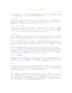
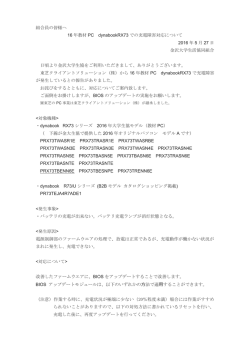
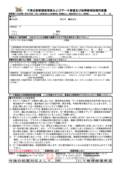
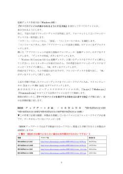
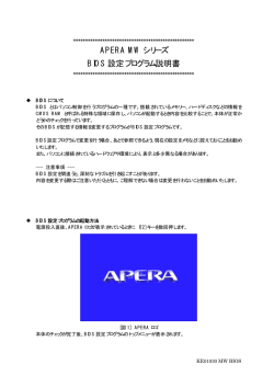
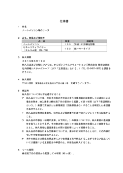
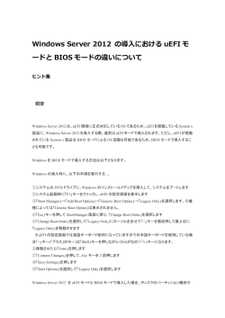
InfoManage 5000SATA Pentium 4 対応タワー型サーバ ユーザーズマニュアル日本語版 Ver. 1.0 コアマイクロシステムズ株式会社 — Introduction 商標 このマニュアルに書かれている製品の仕様や機能は、予告なしに変更されることがあります。 コアマイクロシステムズ(Core Micro Systems)、インフォチップス(InfoTips)、InfoManage の名称と製品 とロゴはコアマイクロシステムズ株式会社の商標です。 Microsoft, Windows, Windows NT, MS-DOS は Microsoft Corporation の商標です。 Intel, Pentium は Intel Corporation の商標です。 このマニュアルのすべての著作権はコアマイクロシステムズにあります。コアマイクロシステムズの許可 なく複製、翻訳、写真複製、印刷、撮影、電子メディア化、電子データ化をすることを禁じます。 © Copyright 2004 Core Micro Systems Inc. All right reserved. This manual version 1.0 2 — Introduction 注意 ① 本書の一部または全部を弊社に無断で転載することは禁止されております。 ② 本書の内容については万全を期しておりますが、万一ご不審の点がございましたら、弊社テクニカルサ ポートまでご連絡くださいますようお願いいたします。 ③ 本製品および本書を運用した結果による損失、利益の逸失の請求等につきましては、②項に関わらず弊 社ではいかなる責任も負いかねますので、あらかじめご了承下さい。 ④ 本書に記載されている機種名、ソフトウェアのバージョンなどは、本書を作成した時点で確認されてい る情報です。本書作成後の最新情報については、弊社テクニカルサポートまでお問い合わせ下さい。 ⑤ 本製品の仕様、デザインおよびマニュアルの内容については、製品改良などのために予告なく変更する 場合があります。 ⑥ 本製品を使用して作成、保存したデータが、ハードウェアの故障、誤動作、その他どのような理由によ って破壊、消失された場合でも、弊社での保証はいたしかねます。万一に備えて、重要なデータはあら かじめバックアップするようにお願いいたします。 ⑦ 弊社は、本製品の仕様がお客様の特定の目的に適合することを保証するものではありません。 ⑧ 本製品は、人命に関わる設備や機器、および高い信頼性や安全性を必要とする設備や機器(医療関係、 航空宇宙関係、輸送関係、原子力関係等)への組み込み等は考慮されていません。これらの設備や機器 で本製品を使用したことにより発生した人身事故や財産損害等など如何なる損失においても弊社では 責任も負いかねます。 ⑨ 本製品は日本国内仕様です。本製品を日本国外で使用された場合、弊社ではいかなる責任も負いかねま す。また、弊社は海外での(海外に対してを含む)サービスおよび技術サポートを行っておりません。 3 — Introduction 注意事項 ************ 安全にお使いいただくために ************ 本製品を安全に正しくご使用いただくために、このマニュアルには安全表示を使用しています。 これらの記載事項は安全のために必ずお守りください。 絵表示について 本製品を正しくご使用いただいて、あなたや他の人々への危害や財産への損害を未然に防止するために、 このマニュアルおよび本製品への安全表示については、以下の絵表示をしています。 この表示を無視して誤った取り扱いをすると、人の死亡 または重傷を負う可能性がある危険が存在する内容を 示しています。 この表示を無視して誤った取り扱いをすると、人が損害 を負う可能性が想定される内容または物理的損害の発 生が想定される内容を示しています。 装置の故障・損傷や誤った操作を防ぐために、操作上必 ず守っていただきたい重要事項や制限事項を示してい ます。 装置を使用する上で、注意すべき、下記人すべきことを 表しています。 4 — Introduction 危 険 / 注 意ラ ベ ル 表 示 に つい て 本製品の外部または内部に黄色地に黒文字で表示されているラベルがあるときは、安全上に関して危険ま たは注意のラベルです。必ず表示の指示に従ってください。 このマニュアルに記載されている以外に危険または注意ラベルによる表示があるときは(例えば製品上に)、 必ずそのラベルによる指示に従ってください。 高温になる場所、湿気の多い場所では使用しないでください。火災や感電の恐れがあります。製品 仕様を確認し、適合した動作環境でご使用ください。 製品の吸気、排気、冷却用の通風口をふさがないよう、10cm以上の空間をあけてください、製品内 に熱が滞留し内部部品発熱による火災の原因となります。 製品にケーブル類を抜き差しする場合には、製品および接続される機器の電源を必ず切断して行っ てください。ケーブルの破損により、火災や感電の原因となります。 本製品を取り扱う場合は、安全の為に、開梱・梱包・移動・設置時には2名以上で作業を行うことを お勧めいたします。 本製品は分解しないでください。分解した状態で使用すると火災や感電の原因となります。 本製品を取り付ける際には、適切に設置してください。振動し易い状態での設置は製品の故障に、 落下し易い状態での設置は事故、怪我の原因となります。 5 — Introduction 振動の発生する場所で使用しないでください。誤動作、故障の原因となります。 急激に温度差を与えると、機器が結露して故障の原因となります。結露させないようにご注意くだ さい。万一、結露させてしまった場合は、1時間以上放置し、完全に乾いたことを確認してからご 使用ください。ただしこの場合の正常動作の保証はできません。 テレビ、スピーカー等、強い電磁気を発生する電子機器の近くに置かないでください。誤動作、故 障の原因となります。 移動する場合は、必ず電源を切り、振動や衝撃を与えないようにしてください。 誤動作、故障の原 因となります。移動する場合には専用梱包箱のご使用をお勧めします。 ホットスワップは、RAIDコントローラが故障と判断したドライブをRAIDアレイから切り離した後に 交換が可能な機能です。 ホットスワップ対応ストレージベイであっても、電源が入った状態で正常動作中のドライブを引き 抜かないでください。 RAIDファームウェアがドライブの取り出しを検知し、ドライブ・ユニットを故障として扱います。 また、動作中の正常なドライブを引き抜いた場合、ドライブ内部のヘッド、ディスクに修復不可能 なダメージを与え、故障の原因となります。 RAIDストレージシステム部において、開梱および移動後に使用する場合には、誤動作を避けるため、 電源を投入する前にドライブを1台ずつ押し込んでください。 本製品には動作確認し、初期化されたドライブを使用しています。弊社が交換部品として提供した ディスク・モジュールのみを交換用として使用してください。 容量やメーカー、型番が同じであっても、弊社提供部品以外のディスクと交換しないでください。 短時間に電源のオン・オフを繰り返さないでください。容量の大きなドライブは内部のディスクの 枚数が多く、その回転が止まるまでに時間がかかります。短い間に電源のオン・オフをすると、止 まりかけたディスクの回転を再度始めることになり、ドライブのスピンドル・モーターやヘッド等 にダメージを与え、寿命を短くする恐れがあります。電源をオフした場合、ドライブ内部のディス クが停止するのにかかる十分な時間(最低約15秒以上)をおいてから、電源をオンしてください。 万一 正常なドライブを取り外すときも同様に、電源をオフしてから十分な時間をおいてから取り外 してください。 RAID装置において、ドライブ障害が発生し、リビルド(データ再構築)動作を実行中に電源のオン・ オフを行わないでください。ドライブへの書き込み中に電源が切断された場合、ドライブ内のデー タ消失やハードウェアの故障につながります。 電源プラグを抜くときは、電源ケーブルを引っ張らないでください。コードが傷つき、火災、感電 の原因となることがあります。必ずプラグを持って抜いてください。 6 — Introduction 設置時のご注意 製品仕様を確認し、設置する環境の温度、湿度が仕様の範囲内であることを確認してください。 振動が多い場所への設置はしないでください。 ラックマウント時、ラックに完全に固定される方法で設置してください。また、ラック内の温度上昇を避けるため、ラック 内各機器間に空間を開け、空気流を妨げない用意してください。 設置後、キャビネットなどの電源アウトレットを利用する場合、本製品の定格が確保できることを確認してください。 本装置の電源インレットは、確実に接地してください。 RAIDストレージシステムは、RAID1, 5などのRAID構成に設定することにより、1台のドライブに障害が 発生してもデータの損失を防ぐよう設計されています。 しかし、2台のドライブに同時に障害が発生した場合や、冗長化されていない部品に障害が発生した場 合はデータが失われる可能性があります。あらかじめご了承ください。また、人為的理由によるデー タの消失、機器の損壊などの理由によりデータを消失する可能性もありますので、重要なデータは必 ず定期的にバックアップをお取りください。 システムが稼働中に、電源を遮断しないでください。ホストコンピュータのメモリやストレージ製品 のキャッシュ・バッファ内に残っているデータが消失し、ファイルやデータが破損する可能性があり ます。緊急の事態以外は、システムのアプリケーション、OSをシャットダウンしてディスク・ドライ ブへのアクセスが停止してから製品の電源を遮断してください。 停電によるデータ消失やシステム障害を避けるために無停電電源(UPS)の使用をお勧めします。 RAID装置において、ドライブ障害が発生し、リビルド(データ再構築)動作を実行中に電源のオン・ オフを行わないでください。 ドライブへの書き込み中に電源が切断された場合、ドライブ内のデータ消失やハードウェアの故障に つながります。 7 — Introduction C h a pt e r 1 Introduction チ ェ ッ ク リス ト InfoManage 5000SATA は、以下の部品を含んでいます。 開封後、全ての部品が揃っているか、破損や故障などがないか確認してください。 InfoManage 5000SATA 本体 AC ケーブル ドライバーCD-ROM フロントパネル用キー×2 マニュアル Pentium 4 (Canterwood) FSB 400/533/800 対応 専用ヒートシンク&背部冷却ファン&エアフローダクト Intel Canterwood Northbridge (E7210)、 Hance Rapids Southbridge (6300ESB)チップセット 最大 4 GB メモリ(DDR 300/333/400 ECC または non-ECC SDRAM) オンボード ATI Rage XL VGA オンボード LAN 10BaseT/100 BaseTX/1000-T Ethernet 対応×2 ホットスワップ対応 SATA/150 HDD トレイ×4 (RAID コントローラオプション) CD-ROM(ATA)、FDD 内蔵 330W 電源 ACPI S0, S1, s4, and S5 規格対応 温度、ファン速度、CPU 速度のハードウェアモニタリング 特徴 8 — Introduction 外観 CD-ROM フロントパネル フロントパネルの LED は、以下のようになっています。 5” メディア スロット ①電源 ②HDD アクセス ③ イ ベ ン ④LAN1 ト ⑤LAN2 ① 電源:サーバの電源が入っているときに点灯します ② HDD アクセス:HDD 読み書き時に点灯します ③ イベント:イベント発生時に点灯します ④ LAN1:LAN1 が接続されているときに点灯します ⑤ LAN2:LAN2 が接続されているときに点灯します フロントパネルは左側が開きます。 フロントパネル用キーでロックすることも可能です。 フロントパネルをロックすると、 ・ 電源スイッチの操作 ・ HDD の取り外し ・ FDD 使用 ・ サイドパネルの開閉、および内部部品取り外し が不可能になります。 フロントパネル用キーは紛失しないように注意してください。 鍵の番号などは当社でも分からないため、再発行はできません。 100V 用電源コネクタ 背面パネル ・100V 用電源コネクタ: 電源ユニット AC ケーブルを接続します。 ・I/O ポート: 詳細は「I/O パネルのポート」をごらんください。 I/O ポート AGP スロット PCI スロット 9 背面冷却ファン — Introduction フロントパネルの開閉と、フロントパネル内部 フロントパネルは左側から開きます。 FDD ホットスワップ HDD ケージ 電源ボタン USB ポート 10 — Introduction HDD トレイの取り付け、取り外し 1.HDD トレイの「○」部分の背面のスイッチを 2.開いたハンドルをさらに引き出すと、HDD ト 引きながらハンドルを引きます。 レイが外れます。 HDD の取り付け、取り外し HDD は、トレイの上にこの写真の向きで左右から 2 本ずつのネジで取り付けます。 HDD は衝撃に弱いコンポーネントです。落としたり、衝撃を与えないよう注意してください。 また、必要が無い場合は取り外さないでください。 11 — Introduction コ ン ポ ー ネン ト の 取 り 付 け ケースの開閉 CPU、メモリの取り外し、PCI/AGP カードの取り付けを行う場合、以下の方法でサーバのケースを開閉 してください。 1. 背面から見て右上と右下にあるネジを緩めます 2.サイドパネルを後ろに 3cm ほどずらします。 (このネジは完全には外れません) 3.サイドパネルの上側をケースから外し、持ち上げ ながら下側もはずします。 12 — Introduction マ ザ ー ボ ード 上 の 部 品 図 1 2 3 4 + + 5 6 32 + + 7 8 31 1 2 3 4 30 9 10 29 11 28 12 27 13 14 15 26 25 24 23 22 21 20 19 18 17 16 図 1 –マザーボード上の部品図 13 — Introduction マザーボード上の部品について詳細 Item Label コンポーネント 参照ページ (1) CPU 取り付けモジュール (2) 478 ピン FC-mPGA2 CPU ソケット (Intel P4/Prescott 対応) (3) 12V PWR CONN 4 ピン 電源コネクタ (4) DIMM1 -4 184-pin DDR SDRAM ソケット (5) PRS 12C CONN 二重化電源ユニット用コネクタ (6) ATX PWR CONN 20 ピン電源コネクタ (7) SECONDARY IDE Secondary IDE コネクタ (8) PRIMARY IDE Primary IDE コネクタ (9) FRONT FAN CONN 前面ファン用電源コネクタ (10) SATA1 SATA コネクタ 1 (11) SATA0 SATA コネクタ 0 (12) USB2 USB (2.0) コネクタ (13) FRONT PANEL フロントパネルコネクタ (14) J1 ジャンパ 1 (15) FDD CONN FDD コネクタ (16) FEATURE CONN フューチャーコネクタ (17) RST BTN リセットボタンコネクタ (18) PWR BTN 電源ボタンコネクタ (19) SCSI LED CONN SCSI LED コネクタ (20) SMBUS CONN IPMB コネクタ (4 ピン) (21) BATTERY CR2032 3V リアルタイムクロック用バッテリ (22) SATA SAF-TE CONN SATA SAF-TE コネクタ (23) J2 Wake-on-LAN (WOL) コネクタ (24) PCI SLOT5 PCI 2.2 スロット 5 (25) PCI SLOT4 PCI 2.2 スロット 4 (26) COM2 CONN シリアルポート COM2 コネクタ (27) PCI SLOT3 (PCI-X) PCI X スロット 3 (28) PCI SLOT2 (PCI-X) PCI X スロット 2 (29) PCI SLOT1 (PCI-X) PCI X スロット 1 (30) AGP CONN APG 4x/8x スロット (31) FRONT FAN CONN ファン用電源コネクタ (32) ×4 22 23 21 24 I/O パネル 15 14 — Introduction I/O パネルのポート S05A の背面 I/O パネルには以下のようなポートが装備されています。 図 2 –I/O ポート PS/2 Mouse PS/2 マウス接続用ポート PS/2 Keyboard PS/2 キーボード接続用ポート USB Ports USB デバイス接続用ポート Parallel Port LPT1 パラレルポート Serial Port COM1 シリアルポート VGA Port VGA ポート LAN Ports 10/100/1000 Mbps RJ-45 LAN ポート(下が LAN1、上が LAN2) I/O ポートの色分け I/O ポートは分かりやすいように標準的な色分けがされています。 コネクタ 色 アナログ VGA 青 パラレルポート ワイン色(赤紫) PS/2 キーボード うすい紫 PS/2 マウス うすい緑 シリアルポート USB 明るい緑(トルコ石) 黒 LAN 黒 15 — Introduction ブ ロ ッ ク ダイ ア グ ラ ム 図 3 –システムブロックダイアグラム この章はここまでです。次章ではコンポーネントのインストール方法について説明します。 16 — Introduction — Notes — 17 C h a pt e r 2 Installing Hardware 安全の為に コンピュータの部品や電子回路は、静電気により破損しやすくなっています。 また、電源に繋がって動作しているコンピュータ内部に触ることは非常に危険です。 死亡、事故、けがを起こさないために、またコンピュータを壊さないように、以下の点に注意してくださ い。 コンピュータ内部の部品取り付けを行うときは、電源ケーブルを抜いてください。電源を繋いだま まだと、感電により死亡、けが、事故の原因となります。 コンピュータ内部の部品取り付けを行うときはアースケーブル付リストストラップを使ってくださ い。同時に、コンピュータの金属部分に触るなどして、なるべく静電気を逃がし、コンピュータ内 部部品に静電気が加わらないようにしてください。静電気がマザーボードを含めたコンピュータ部 品に加わると、故障や破損の原因となります。 マザーボードを含めた電子部品の基板回路や金属端子、部品は触らないようにしてください。基盤 の端の部分を持ち、基板や部品に力を加えないように取り付けてください。 取り付ける前の部品、また取り外した部品は静電気防止袋に入れて保管してください。 — Installing Hardware マ ザ ー ボ ード の ジャ ン パ 設 定 このセクションではマザーボード上のジャンパを設定する方法について説明します。 ジャンパの設定 ジャンパ設定によりマザーボードの設定の変更が可能です。ジャンパは「ジャンパピン」に「ジャンパキ ャップ」を付けることにより設定されます。 2 ピンのジャンパピンにジャン パキャップを付けた状態。 「ジ ャンパ ON」または「ジャンパシ ョート」と呼びます。 2 ピンのジャンパピンからジャ ンパキャップを外した状態。 「ジャンパ OFF」または「ジ ャンパオープン」と呼びます。. 3 ピン以上のジャンパピンの場 合、どのピンにジャンパキャッ プを付けるかによって設定が 変わります。この図のように 1 と 2 にジャンパキャップを付け た場合、 「1 と 2 をジャンパシ ョートした」と言います。 1 2 3 20 — Installing Hardware マザーボードのジャンパ設定 ジャンパの設定は以下の通りになっています。 図 4 –ジャンパ 1 ピン 機能 出荷時設定 1-2 パスワードを使用 する OFF/オープン 3-4 NVRAM クリア OFF/オープン 21 — Installing Hardware CP U の 取 り 付 け 13 ページのイラストを参照して、CPU ソケットの場所を確認してください。 以下のイラストを確認し、CPU を取り付けます。 1. CPU ソケットのロックレバーを引きあげてください。 2. CPU ソケットと CPU の 1 番ピンの位置を確認してください。 3. CPU ソケットと CPU の 1 番の位置を合わせ、真上から、斜め にならないように CPU をソケットに取り付けてください。 下記「注意事項」を読んでください。 4.CPU ソケットのロックレバーをロックされる位置まで下げてく ださい。 注意事項 FC-PGA2, 478 ピン ソケットは ZIF ソケット(Zero Insertion Force socket)です。このタイプのソケ ットは簡単に CPU が取り付けられるようになっています。CPU をソケットの上に置くだけで簡単 にソケットに入り、ロックレバーを下げると CPU を固定されます。もしもソケットの上に CPU を 置いても CPU がソケットから浮いている場合や、CPU をソケットに取り付けるときに簡単に入ら ない場合などは、CPU の向きを間違えているか、CPU のピンが曲がっているか、ロックレバーが 上がっていない可能性があります。取り付けを再度確認してください。 22 — Installing Hardware メ モ リ の 取り 付 け このマザーボードはメモリモジュールを取り付けるために 4 つの DDR DIMM(Double Data Rate Dual In-line Memory Modules)スロットを装備しています。メモリモジュールは 2.5V DDR SDRAM メモリチ ップが必要です。 メモリの取り付けは、以下の手順で行ってください。 1. DIMM スロットの両端にあるロックラッチを外側に開き、メモリと DIMM ソケットの切り欠きの位置を 確認してください。 2. 斜めにならないよう注意し、DIMM ソケットにメモリを軽く入れてください。 3. メモリが正しく DIMM スロットに入っていることを確認したら、DIMM スロットにメモリをさらに 押し込んでください。ロックラッチが内側に戻り、メモリを固定します。 23 — Installing Hardware P CI カ ー ド の 取 り 付 け 13 ページのイラストを参照して、CPU ソケットの場所を確認してください。 以下のイラストを確認し、CPU を取り付けます。 1. 2. コンピュータケースのブランクプレート(鉄板の蓋)をはずしてください。 斜めにならないよう注意し、PCI カードを PCI 拡張スロットに差し込みます。 3. ネジで PCI カードをコンピュータケースに固定してください。 この章はここまでです。次章では BIOS 設定方法について説明します。 24 — Installing Hardware — Notes — 25 C h a pt e r 3 BIOS 設 定 メ ニ ュー このマザーボードは最新の AMI BIOS CMOS チップを搭載し、Windows プラグ&プレイをサポートして います。この CMOS チップは、マザーボードの BIOS (Basic Input and Output System)を設定するため の機能を持っています。 「BIOS Setup Utility (BIOS 設定ユーティリティ)」はコンピュータ(マザーボード)の設定を変更し、個別 のニーズにあわせたシステム設定に変更するための設定メニューです。 BIOS Setup Utility を起動すると、コンピュータの設定状態が表示され、各種の設定変更が可能です。設 定内容は CMOS の RAM に保存され、バッテリーによりバックアップされるのでコンピュータの電源をオ フにしても消えないようになっています。コンピュータの電源を入れると、CMOS から設定内容を呼び出 し、その設定に従い起動します。 BIOS Setup Utility の主な機能は以下の通りになっています。 HDD、FDD などのドライブ類、USB や COM などのポート設定変更と保存 BIOS 設定のパスワードによる保護 パワーマネジメント機能設定 BIOS Setup Utility は以下のような場合に使用してください。 コンピュータの設定を変更する時 「make changes to the Setup utility」(BIOS Setup Utility で設定を変更してください)エラーが発生した 時 IRQ やシリアルポート番号などのコンフリクト(番号の衝突)を避けるために設定変更する時 パワーマネジメント設定を変更する時 BIOS 設定用パスワードの変更や、その他のセキュリティ設定をする時 注意: BIOS Setup Utility 画面で、[]で囲まれている項目のみが設定変更可能項目です。 BIOS Setup Utility を起動する方法 コンピュータの電源を入れてすぐに画面に「<DEL> Enter the BIOS Setup」と表示されます。ここで Delete キーを押すと、BIOS Setup Utility が起動します。 — BIOS Main (メインメニュー) 「Main」のメニューでは、マザーボードと BIOS の現在の情報(状態)が表示されます。 BIOS SETUP UTILITY Main Advanced BIOS Version Power Boot Security Exit BIOS Build Date Processor Type : S05A3A11 : 03/02/04 : Intel® Pentium 4® CPU 2.80GHz Front Side Bus Speed Processor Speed CPU ID Level 1 Cache Level 2 Cache Total Memory : 800 MHz : 2.8 GHz : F33 16KB 1024KB 512MB System Time System Date ←→ ↑↓ Enter [23:36:32] [Tue 03/30/2004] F1 F9 F10 ESC Select Screen Select Item Go to Sub screen General Help Load Defaults Save and Exit Exit V02.48 ©Copyright 1985-2002, American Megatrends Inc. BIOS Version: BIOS のバージョンが表示されます。 BIOS Build Date: BIOS の作成日が表示されます。 マザーボードに取り付けられた CPU の情報が表示されます。 Processor Type: Front Side Bus Speed: FSB(CPU の最大データ転送速度を表す項目)のクロック数が表示されます。 Processor Speed: CPU の動作速度が表示されます。 CPU ID: CPU の ID コードが表示されます。 Level 1 Cache: CPU の内部 L1 キャッシュ容量が表示されます。 Level 2 Cache: CPU の内部 L2 キャッシュ容量が表示されます。 Total Memory: メインボードに取り付けられたメモリの容量が表示されます。 System Time: RTC (リアルタイムクロック。コンピュータ内部の時計) に設定された現在の時間が表示さ れます。スクロールすることにより設定変更可能です。 System Date: RTC に設定された現在の日付が表示されます。スクロールすることにより設定変更可能です。 28 — BIOS Advanced (アドバンストメニュー) このメニューでは、コンピュータの高度な設定が可能です。 注意! アドバンストメニューの設定項目について、間違えた設定を行うとコンピュータが起動しなくなる可能性があります。 このような BIOS の高度な設定について知識と経験が無い場合、むやみに設定を変更しないことをお勧めいたします。 設定ミスによりコンピュータが誤動作する場合、または正常に起動しなくなった場合は、BIOS Setup Utility の” Exit” メニューから"Load Optimal Defaults"を選択してください。 BIOS SETUP UTILITY Main Advanced Power Boot Security Exit Setup Warning Setting items on this screen to incorrect values May cause the system to malfunction! ► Super IO Configuration ► IDE Configuration ► Floppy Configuration ► PCIPnP Configuration ► Boot Setting Configuration ► Onboard Devices Configuration ► Event Log Configuration ► Remote Access Configuration ► System Health Monitor ←→ ↑↓ Enter F1 F9 F10 ESC Select Screen Select Item Go to Sub screen General Help Load Defaults Save and Exit Exit V02.48 ©Copyright 1985-2002, American Megatrends, Inc. ‘ ►’がついている項目は、サブメニューがあることを意味しています。カーソルで項目を上下し、Enter キーを押すことによりそれぞれのメニューが表示されます。 29 — BIOS Super IO Configuration (I/O ポートチップセット設定) この項目を選択し、<Enter>を押すと以下の画面が表示されます。 SuperIO Chipset Nat373 Advanced Configure Nat373 Super IO Chipset ___________________________________________________ Serial Port1(Address/IRQ): Serial Port2(Address/IRQ); Parallel Port Address Parallel Port Mode ECP Mode DMA Channel Parallel Port IRQ [3F8/IRQ4] [Disabled] [378] [ECP] [DMA3] [IRQ7] ←→ ↑↓ Enter F1 F9 F10 ESC Select Screen Select Item Go to Sub screen General Help Load Defaults Save and Exit Exit V02.48 ©Copyright 1985-2002, American Megatrends, Inc. Serial Port 1(Address/IRQ): オンボードシリアルポート(COM1)の I/O アドレス、IRQ の設定変更する項 目です。 Serial Port 2(Address/IRQ): 使用しないので[Disabled]に設定します。 Parallel Port Address: オンボードパラレルポート(LPT)の I/O アドレスを設定変更する項目です。 Parallel Port Mode: オンボードパラレルポート(LPT)のモードを設定変更する項目です。モードは 4 種類 あり、Normal, Bi-Directional, EPP (Enhanced Parallel Port), ECP (Extended Capabilities Port)となっ ています。プリンタなどのパラレルポート接続機器が Normal モード以外へ設定しないと動作しない場合 は変更をしてください。 ECP Mode DMA Channel: オンボードパラレルポート(LPT)を ECP モードに設定したときに、DMA チャ ンネルの設定を DMA 3 (工場出荷時はこの設定です)と DMA 1 から選択する項目です。 Parallel Port IRQ: オンボードパラレルポート(LPT)の IRQ を設定変更する項目です。 30 — BIOS IDE Configuration (IDE HDD 設定) この項目を選択し、<Enter>を押すと以下の画面が表示されます。 BIOS SETUP UTILITY Advanced DISABLED: disables the IDE Configuration --------------------------------------------------------------------------------- Integrated IDE Controller. IDE Configuration [P-ATA Mode] P-ATA: enables only the P-ATA IDE S-ATA Running Enhanced Mode [Disabled] Controller. S-ATA: enables ► Primary IDE Master [Hard Disk] only the S-ATA IDE ► Primary IDE Slave [Not Detected] Controller. ► Secondary IDE Master [ATAPI CDROM] Combined: 4 Hard Drive ► Secondary IDE Slave [Not Detected] ► Third IDE Master [Hard Disk] SATA Hard Drive use as ► Fourth Slave [Not Detected] P-ATA Channel ←→ ↑↓ +F1 F9 F10 ESC Select Screen Select Item Change Option General Help Load Defaults Save and Exit Exit V02.48 ©Copyright 1985-2002, American Megatrends, Inc. IDE Configuration: オンボード IDE コントローラを設定変更する項目です。3 つの選択項目があります。 Disabled: IDE デバイスを使用しない設定で す。 P-ATA Mode: P-ATA(Parallel ATA)の IDE デバイ スを使用する設定です。 Combined 2 つの P-ATA と、2 つの S-ATA(Serial Mode: ATA)を使用する設定です。 S-ATA Running Enhanced Mode: Enable, Disable の、2 つの選択項目があります。 Enabled に設定すると、最大 4 つの P-ATA デバイスと 2 つの S-ATA デバイスをサポートします。 Primary/Secondary/Third IDE Master/Slave: IDE チャンネルに接続された各 IDE デバイスを設定変更す る項目です。このマザーボードには (Primary, Secondary, third, forth)の 4 つの IDE チャンネルがあります。 そのうち Primary と Secondary の2つのチャンネルには、Master と Slave 設定により最大 2 つづつデバイ スが接続可能です。つまり、Primary-Master, Primary-Slave, Secondary-Master, Secondary-Slave と、最大 4 つのデバイスが接続可能です。 31 — BIOS IDE Configuration が[P-ATA Mode]で、S-ATA Running Enhanced mode が[Enabled](使用する) の設 定 BIOS SETUP UTILITY Advanced IDE configuration IDE Configuration [P-ATA Mode] S-ATA Running Enhanced Mode [Enabled] S-ATA Ports Definition [P0-3rd. M/P1-4th.M] ► Primary IDE Master ► Primary IDE Slave ► Secondary IDE Master ► Secondary IDE Slave ► Third IDE Master ► Forth IDE Master [Hard Disk] [Not Detected] [ATAPI CDROM] [Not Detected] [Hard Disk] [Not Detected] DISABLED: disables the Integrated IDE Controller. P-ATA: enables only the P-ATA IDE Controller. S-ATA: enables only the S-ATA IDE Controller. Combined: enables both IDE Controllers. ←→ ↑↓ +F1 F9 F10 ESC Select Screen Select Item Change Option General Help Load Defaults Save and Exit Exit V02.48 ©Copyright 1985-2002, American Megatrends, Inc IDE Configuration: IDE Configuration が[P-ATA Mode]になっていると P-ATA IDE が使用できます。同 時に S-ATA Enhanced Mode が[Enabled]になっているので、最大 4 つの P-ATA デバイスと 2 つの S-ATA デバイスが使用可能です。 S-ATA Running Enhanced Mode: [Enabled](使用する)と[Disabled](使用しない)の、2 つの選択項目が あります。 Enabled にすると、最大 4 つの P-ATA デバイスと 2 つの S-ATA IDE デバイスが使用可能です。 S-ATA Ports Definition: S-ATA ポートの設定を変更する項目です。 P0-3rd.M / P1-4th.M: S-ATA ポート 0 を Third Master に、S-ATA ポート 1 を Forth Master に設定します。 P1-3th.M / P0-4th.M: S-ATA ポート 1 を Third Master に、ポート 0 を Forth Master に設 定します。 Primary/Secondary IDE Master/Slave: IDE チャンネルに接続された各 IDE デバイスを設定変更する 項目です。このマザーボードには (Primary, Secondary, third, forth)の 4 つの IDE チャンネルがありま す。そのうち Primary と Secondary の2つのチャンネルには、Master と Slave 設定により最大 2 つづ つデバイスが接続可能です。つまり、Primary-Master, Primary-Slave, Secondary-Master, Secondary-Slave と、最大 4 つのデバイスが接続可能です。 Third/Fourth IDE Master/Slave: 残り 2 つのチャンネルの IDE デバイスを設定変更する項目です。 32 — BIOS IDE Configuration が[Combined Mode]の設定 BIOS SETUP UTILITY Advanced P-ATA 1st Channel : IDE configuration IDE Configuration Combined Mode Option S-ATA Ports Definition [Combined Mode] [P-ATA 1st Channel] [P0-Master/P1-Slave] ► Primary IDE Master ► Primary IDE Slave ► Secondary IDE Master ► Secondary IDE Slave ► Third IDE Master ► Forth IDE Master [Not Detected] [Not Detected] [Not Detected] [Not Detected] [Hard Disk] [Not Detected] P-ATA as Fist Channel S-ATA as Second Channel ←→ ↑↓ +F1 F9 F10 ESC Select Screen Select Item Change Option General Help Load Defaults Save and Exit Exit V02.48 ©Copyright 1985-2002, American Megatrends, Inc. IDE Configuration: IDE Configuration が[Combined Mode]に設定されているときには、2 つの P-ATA と 2 つの S-ATA が使用可能です。 Combined Mode Option: 最初のチャンネルに P-ATA と S-ATA のどちらを割り当てるのか設定変更 する項目です。 S-ATA Ports Definition: S-ATA ポート 0 と 1 の Master/Slave 割り当てを設定変更する項目です。 P0-Master/P1-Slave: S-ATA ポート 0 を Master に、S-ATA ポート 1 を Slave に設定します。 P0-Slave/P1-Slave: S-ATA ポート 0 を Slave に、S-ATA ポート 1 を Master に設定します。 33 — BIOS IDE HDD の設定 (Primary IDE Master に HDD が接続されている例) BIOS SETUP UTILITY Advanced Primary IDE Master ___________________________________________________ Device : Hard Disk Vendor : IBM-DTTA-351010 Size : 10.1GB LBA Mode : Supported Block Mode : 16Sectors PIO Mode : 4 Async Mode : MultiWord DMA-2 Ultra DMA : Ultra DMA-2 S.M.A.R.T. : Supported ____________________________________________________ Type [Auto] LBA/Large Mode [Auto] Block Mode [Auto] PIO Mode [Auto] DMA Mode [Auto] S.M.A.R.T. [Auto] 32Bit Data Transfer [Disabled] ←→ ↑↓ +F1 F9 F10 ESC Select Screen Select Item Change Option General Help Load Defaults Save and Exit Exit v02.48 ©Copyright 1985-2002, American Megatrends, Inc. Primary IDE Master: Primary IDE に設定されたデバイスの情報が表示されます。この例では HDD の情 報が表示されています。各情報は以下のようになっています。 Device: 取り付けられているデバイスの種類が表示されます Vendor: デバイスの名称が表示されます Size: デバイスの容量が表示されます LBA Mode: LBA (Logical Block Addressing)モードをサポートしているか表示されます (LBA モード とは 504GB より大きい容量の HDD を使用するときに使う機能です) Block Mode: ブロックのセクタ数が表示されます PIO Mode: PIO モードの設定値が表示されます Async Mode: DMA チャンネルの Async(非同期)モード設定値が表示されます Ultra DMA: Ultra DMA モードの設定値が表示されます S.M.A.R.T.: S.M.A.R.T モードをサポートしているか表示されます Type: [Enabled]を選択すると HDD の設定が変更可能です。[Auto]を選択すると BIOS が取り付けられて いる IDE デバイスを自動で検出し、設定をします。 LBA/Large Mode: [Enabled]を選択すると LBA モードに設定されます。[Auto]を選択すると BIOS が IDE デバイスの LBA モード対応を検出し、設定します。 Block Mode: 取り付けられている HDD がブロックモードに対応している場合[Enabled]を選択してくださ い。BIOS がブロックサイズを検出し設定を行い、IDE デバイスへのアクセス速度が高速化します。 PIO Mode: 各 IDE チャネルには、それぞれ master と slave のデバイスが接続可能です。これらの各 IDE デバイスに、使用する PIO (Programmed Input/Output)モードを 0-4 から選択可能です。[Auto]を選択す 34 — BIOS ると BIOS は最適な PIO モードを検出し、設定します。 DMA Mode: このマザーボードは UltraDMA に対応し、高速な IDE アクセスデバイスが可能になってい ます。取り付けた IDE デバイスが UltraDMA に対応している場合、[Auto]に設定することによりマザーボ ードは UltraDMA データ転送を行います。 S.M.A.R.T: 機 器 の 状 態 を 監 視 し 、 パ フ ォ ー マ ン ス 予 測 を 行 い 、 診 断 を 行 う の が S.M.A.R.T. (Self-Monitoring, Analysis, and Reporting Technology)です。S.M.A.R.T. を実行するソフトウェアは HDD とコンピュータの両方にあります。 HDD のソフトウェアは内部モーター、メディア、ヘッド、電子部品のパフォーマンス、をモニターします。 コンピュータのソフトウェアは HDD 全体の信頼性について状態を監視します。 デバイスの不具合が予想された場合、ホストのソフトウェアは S.M.A.R.T アプレットを通じてユーザに状 況を報告し、データ保護をするようアドバイスします。 32-Bit Data Transfer: 32 ビットデータ転送の設定を行います。IDE デバイスが 32 ビットデータ転送に対 応しているときには[Enable]に設定します。 35 — BIOS Floppy Configuration (フロッピーディスクドライブの設定) この項目を選択し<Enter>を押すと以下のような画面が表示されます。 BIOS SETUP UTILITY Advanced Floppy Configuration Select the type of ____________________________________________________ floppy drive connected to the Floppy A [1.44MB 31/2”] system. ←→ ↑↓ +F1 F9 F10 ESC Select Screen Select Item Change Option General Help Load Defaults Save and Exit Exit V02.48 ©Copyright 1985-2002, American Megatrends, Inc Floppy A: 取り付けられているフロッピーディスクにあわせて設定をします。工場出荷時は Floppy A に” が取り付けられている設定になっています。 3.5-inch, 1.44 MB€35 36 — BIOS PCI PnP Configuration (PCI プラグ&プレイ設定) この項目を選択し<Enter>を押すと以下のような画面が表示されます。 BIOS SETUP UTILITY Advanced Plug & Play O/S Reset Resource Assignment PCI Latency Timer [No] [No] [64] USB Function Legacy USB Support [Enable] [AUTO] PCI Slot-1 IRQ PCI Slot-2 IRQ PCI Slot-3 IRQ PCI Slot-4 IRQ PCI Slot-5 IRQ [9] [9] [9] [Auto] [Auto] Preference Preference Preference Preference Preference ←→ ↑↓ +F1 F9 F10 ESC Select Screen Select Item Change Option General Help Load Defaults Save and Exit Exit V02.48 ©Copyright 1985-2002, American Megatrends, Inc. Plug & Play O/S: プラグ&プレイ対応 OS によってプラグ&プレイ対応デバイスを設定させたい場合” Yes” に設定します。BIOS によってプラグ&プレイ対応デバイスを設定させたい場合は” No” に設定します。 Reset Resource Assignment: この項目を[Yes]にすると、再起動後に BIOS に保存されたプラグ&プレイ設 定データは消去され、新しく更新されたデータが作成されます。 PCI Latency Timer: PCI カードがここで指定されたクロックでバスにアクセスします。他のデバイスから もアクセス要求がある時に、デバイスが PCI バスをどのくらい占有できるか設定することが可能です。 USB Function: オンボード USB 機能の設定が変更可能です。USB デバイスを接続しない場合は disable に設定し、リソースを開放することができます。 Legacy USB Support: レガシーOS(DOS 等)で USB デバイスを使用する場合は Enable に設定してくださ い。 PCI Slot-1/2/3/4/5 IRQ Preference: [Auto]に設定すると各 PCI スロットに接続した PCI デバイスの IRQ を自動設定します。 37 — BIOS Boot Settings (起動設定) この項目を選択し<Enter>を押すと以下のような画面が表示されます。 BIOS SETUP UTILITY Advanced Boot Setting Configuration --------------------------------------------------------------------------------Quick Boot [Enabled] Quiet Boot [Enabled] --------------------------------------------------------------------------------Hyper-Threading [Enabled] Auto-detect CPU Frequency [Enabled] Bootup Num-Lock [On] PS/2 Mouse Support [Auto] Parity Check [Enabled] Wait ‘ F1’If Error [Enabled] MPS 1.4 Support [Enabled] ASF Support [Enabled] ←→ Select Screen ↑↓ Select Item +Change Option F1 General Help F9 Load Defaults F10 Save and Exit ESC Exit V02.48 ©Copyright 1985-2002, American Megatrends, Inc. Boot Setting Configuration: コンピュータ起動時の設定を選択する項目です。 Quick Boot: [Enabled]に設定すると起動時の POST テストを行わないため、高速に起動するようになりま す。 Quiet Boot: [Enabled]に設定すると、起動時のメモリテストで音を鳴らしません。 Hyper-Threading: [Enabled]に設定すると、Hyper Threading 機能が使用できます。Hyper Threading を 使用すると、物理的には 1 つの CPU が論理的な複数の CPU として表示されます。(Hyper Threading に 対応した CPU と OS で使用可能です) Auto-detect CPU frequency: [Enabled]に設定すると、CPU の周波数が自動的に検出されます。 Bootup Num-Lock: [ON]に設定すると、起動時にキーボードのテンキー部がテンキーとして認識されます。 [Off]にすると、テンキー部をカーソルキーとして扱います。 PS/2 Mouse Support: PS/2 マウスを使用するときは[Enabled]に設定してください。 Parity Check: [Enabled]に設定すると、システムはメモリを完全にチェックします。 Wait ‘ F1’ If Error: [Enabled]に設定すると、起動時にエラーが発生した場合” Press the F1 key to continue€35 のメッセージが表示されます。 MPS 1.4 Support: [Enabled]に設定すると、Pentium CPU を使った SMP ベースの PC において Intel の Multi Processing 機能に対応します。 ASF Support: [Enabled]に設定するとネットワークで Windows Active Streaming Format によるオーデ ィオ、ビデオ配信に対応します。 38 — BIOS Onboard Devices Control Configuration (オンボードデバイスの設定) この項目を選択し<Enter>を押すと以下のような画面が表示されます。 BIOS SETUP UTILITY Advanced Use this question to Special onboard devices configuration settings ------------------------------------------------------------------------------------- Enable/Disable Onboard Gigabit LAN. Onboard LAN 1 [Enabled] Onboard LAN 2 [Enabled] Onboard PCI VGA [Auto] ←→ ↑↓ +F1 F9 F10 ESC Select Screen Select Item Change Option General Help Load Defaults Save and Exit Exit V02.48 ©Copyright 1985-2002, American Megatrends, Inc. Onboard LAN1/2: オンボードのネットワークコントローラ(LAN1/ 2)の使用設定を行います。背面の RJ-45LAN コネクタで LAN 接続を使用するのであれば[Enabled]に設定します。 Onboard VGA Device: オンボードビデオコントローラの使用設定を行います。背面の VGA コネクタでデ ィスプレイ表示を使用するのであれば[Auto]に設定します。 39 — BIOS Event Log Configuration (イベントログ設定) この項目を選択し<Enter>を押すと以下のような画面が表示されます。 BIOS SETUP UTILITY Advanced Event Logging details ------------------------------------------------------------------------------------View Event Log Clear Event Log Event Log Statistics Event Control Interface BIOS POST Event Logging ECC Event Logging PCI Device Event Logging AC Power Lost/Recovery Intrusion Event Logging Front Fan Event Logging Rear Fan Event Logging [Enabled] [Enabled] [Enabled] [Disabled] [Enabled] [Enabled] [Enabled] View all unread events on the Event Log. ←→ ↑↓ +F1 F9 F10 ESC Select Screen Select Item Change Option General Help Load Defaults Save and Exit Exit V02.48 ©Copyright 1985-2002, American Megatrends, Inc. View Event Log: イベントログ内の未読イベントを表示します。 Clear All Event Log: イベントログ内の全てのイベントを消去します。 Event Log Statistics: 未読イベントの数について詳細を表示します。 Event Control Interface: BIOS POST Event Logging: BIOS POST エラーをログに残す場合[Enabled]にします。 ECC Event Logging: シングルビット/マルチビット ECC メモリエラーをログに残す場合[Enabled]にします。 PCI Device Event Logging: PCI デバイスエラーをログに残す場合[Enabled]にします。 AC Power Lost/Recovery: AC 電源の状態をログに残す場合[Enabled]にします。 Intrusion Event Logging: シャーシ状態をログに残す場合[Enabled]にします。 Front Fan Event Logging: 前面ファンの状態をログに残す場合[Enabled]にします。 Rear Fan Event Logging: 背面ファンの状態をログに残す場合[Enabled]にします。 40 — BIOS Remote Access Configuration (リモートアクセスの設定) この項目を選択し<Enter>を押すと以下のような画面が表示されます。 BIOS SETUP UTILITY Advanced Configure Remote Access type and parameters ____________________________________________________ Remote Access [Serial] Serial port number Serial Port Mode Post-Boot support [COM1] [115200 8,n,1] [Disabled] Terminal Type Flow Control [ANSI] [None] Select Remote Access type. ←→ ↑↓ +F1 F9 F10 ESC Select Screen Select Item Change Option General Help Load Defaults Save and Exit Exit V02.48 ©Copyright 1985-2002, American Megatrends, Inc. Remote Access: [Enabled]に設定すると、リモートアクセスにシリアルポートが使用できます。 Serial port number: 使用するシリアルポートの番号を選択します。 Serial Port Mode: リモートアクセスに使用するポートの通信速度、プロトコルを設定します。 Post Boot support: DOS から起動した後リモートアクセスを可能にします。 Terminal Type: ターミナルモードを選択します。 Flow Control: コンソールリダイレクトのフローコントロールを設定します。 41 — BIOS System Health Monitor (システム状態の監視) この項目を選択し<Enter>を押すと以下のような画面が表示されます。 BIOS SETUP UTILITY Advanced System Health Details ____________________________________________________ CPU1 Temperature System Temperature = 35°/95°F = 28°/82°F Rear Fan Speed Front Fan Speed 1500 RPM 1140 RPM Reset Chassis Status ► Voltage Monitor [Disabled] ←→ ↑↓ +F1 F9 F10 ESC Select Screen Select Item Change Option General Help Load Defaults Save and Exit Exit V02.48 ©Copyright 1985-2002, American Megatrends, Inc.. CPU temperature: CPU 温度を表示します。 System Temperature: システム内部温度を表示します。 Rear Fan Speed: 背面ファンの回転速度を表示します。 Front Fan Speed: 前面ファンの回転速度を表示します。 Voltage Monitor: 電圧監視サブ画面を表示します。 42 — BIOS BIOS SETUP UTILITY Advanced Voltage Monitor ____________________________________________________ Vbat 5.0 V -12 V 12 V CPU Vcore Vtt (MCH) Vtt (DDR) 1.5 V 2.6 V 3.3 V 3.3 Vsb 5.0 Vsb 1.2 V (LAN) 1.8 V (LAN) 2.5 V (VGA) = 3.0560 V = 4.8880 V =-12.1650 V = 12.0625 V = 1.5000 V = 1.4880 V = 1.3320 V = 1.5360 V = 2.6760 V = 3.3408 V = 3.3408 V = 5.2480 V = 1.2700 V = 1.8200 V = 2.5600 V ←→ ↑↓ +F1 F9 F10 ESC Select Screen Select Item Change Option General Help Load Defaults Save and Exit Exit V02.48 ©Copyright 1985-2002, American Megatrends, Inc. Voltage Monitor: 各部、各電圧状態を表示します。 43 — BIOS Power (電源の設定) この項目を選択し<Enter>を押すと以下のような画面が表示されます。 BIOS SETUP UTILITY Main Advanced Power Boot Security Power Button Mode AC Lose Handling [Instant On/Off] [Last State] Standby Time Out [Disabled] Exit Instant On/Off: Power On or Off the system when power button is pressed. ←→ Select Screen ↑↓ Select Item +Change Option F1 General Help F9 Load Defaults F10 Save and Exit ESC Exit v02.48 ©Copyright 1985-2002, American Megatrends, Inc.. Power Button Mode: ACPI(Advanced Configuration and Power management Interface)設定時、ソフト ウェア的な電源切断が可能です。この状態ではウェイクアップアラームと共にシステムを再開します。こ の時電源ボタンはシステムの通常電源切断として使用するためのソフトウェアをインストールさせます。 [Instant On/Off]に設定されているとき、電源ボタンはソフトウェア電源切断として機能します。 [4 Sec. Override]に設定されているとき、ソフトウェア電源切断するために電源ボタンを 4 秒間押しつづけ る必要があります。 AC Power Failure:予期しない電源切断によるシステム停止後の設定を行います。 Standby Time Out: スタンバイ時のパワーセーブモードへの以降時間を分単位で設定します。 44 — BIOS Bo o t ( 起 動 デ バ イ ス の 設 定 ) この項目を選択し<Enter>を押すと以下のような画面が表示されます。 BIOS SETUP UTILITY Main Advanced Power Boot Security Exit ---------------------------------------------------------------------------------► Boot Device Priority ► Hard Disk Drivers ► Removable Devices ► ATAPI CDROM Drives ←→ Select Screen ↑↓ Select Item +Change Option F1 General Help F9 Load Defaults F10 Save and Exit ESC Exit V02.48 ©Copyright 1985-2002, American Megatrends, Inc. Boot Device Priority: コンピュータ起動時の起動デバイスについて順番を設定します。Enter を押すとサ ブメニューが表示されます。 Removable Devices: 取り付けられているリムーバブルデバイスを表示します。 ATAPI CDROM Drives: 取り付けられている CD-ROM デバイスを表示します。 45 — BIOS Boot Devices Priority BIOS SETUP UTILITY Boot Boot Devices Priority -----------------------------------------------------------------------------------1st Boot Device 2nd Boot Device 3rd Boot Device 4th Boot Device [1st Floppy Drive] [ATAPI CDROM] [Hard Disk] [IBA GE Slot 0420 v] ←→ ↑↓ +F1 F9 F10 ESC Select Screen Select Item Change Option General Help Load Defaults Save and Exit Exit v02.48 ©Copyright 1985-2002, American Megatrends, Inc ここで起動デバイスの順番を設定します。 46 — BIOS Removable Devices BIOS SETUP UTILITY Boot Boot Devices Priority -----------------------------------------------------------------------------------1st Removable Device [1st Floppy Drive] ←→ ↑↓ +F1 F9 F10 ESC Select Screen Select Item Change Option General Help Load Defaults Save and Exit Exit V02.48 ©Copyright 1985-2002, American Megatrends, Inc. リムーバブルデバイスが表示されます。 47 — BIOS ATAPI CD-ROM Drives BIOS SETUP UTILITY Boot ATAPI CD-ROM Drives -----------------------------------------------------------------------------------ATAPI CDROM Drive [PM-CD-RW-CDR-7S52] ←→ ↑↓ +F1 F9 F10 ESC Select Screen Select Item Change Option General Help Load Defaults Save and Exit Exit v02.48 ©Copyright 1985-2002, American Megatrends, Inc. CD-ROM が表示されます。 48 — BIOS Security (セキュリティの設定) この項目を選択し<Enter>を押すと以下のような画面が表示されます。 BIOS SETUP UTILITY Main Advanced Supervisor Password User Password Power Boot Security : Not Installed : Not Installed Exit Install or Change the password. Change Supervisor Password Change User Password ←→ ↑↓ Enter F1 F9 F10 ESC Select Screen Select Item Change General Help Load Defaults Save and Exit Exit v02.48 ©Copyright 1985-2002, American Megatrends, Inc. Supervisor Password: スーパーバイザーのパスワードが設定されているか表示されます。 User Password: ユーザーパスワードが設定されているか表示されます。 Change Supervisor Password: スーパーバイザーのパスワードを設定します。 Change User Password: ユーザーパスワードを設定します。 ・ ユーザーパスワードを設定するには、スーパーバイザーパスワードが設定されてい る必要があります。 ・ ユーザーパスワード権限では Setup Utility の設定変更はできません。 ・ パスワードの最大文字数は 6 文字です。 ・ パスワード入力後、確認のため再度パスワードを入力する必要があります。 ・ 起動時、または Setup Utility 起動時にパスワード入力が求められます。 49 — BIOS Exit (Setup Utility の終了) この項目を選択し<Enter>を押すと以下のような画面が表示されます。 BIOS SETUP UTILITY Main Advanced Power Boot Security Exit Exit system setup After saving the changes. Save Changes and Exit Discard Changes and Exit Load Optimal Defaults Discard Changes F10 key can be used for this operation. ←→ Select Screen ↑↓ Select Item Enter Go to Sub Screen F1 General Help F9 Load Defaults F10 Save and Exit ESC Exit v02.48 ©Copyright 1985-2002, American Megatrends, Inc. Save Changes and Exit: Setup Utility で変更した全ての項目を BIOS に保存し、Setup Utility を終了す る時にこの項目を選択して Enter を押してください。 確認のダイアログボックスが表示され、” を押すと保存されます。” を押すとこの画面に戻ります。 Y” N” Discard Changes and Exit: Setup Utility で変更した全ての項目を破棄し、BIOS には何も変更を保存せず Setup Utility を終了するときにこの項目を選択して Enter を押してください。 確認のダイアログボックスが表示され、” を押すと保存せず終了します。” を押すとこの画面に戻りま Y” N” す。 Load Optimal Defaults: BIOS に保存されている最善状態の設定を呼び出す時にこの項目を設定して Enter を押してください。 確認のダイアログボックスが表示され、” Y” を押すと最善状態が呼び出されます。” N” 「最善状態設定」にした場合、遅いメモリやコンポーネントを使用している場合、起動しない場合がありま す。. Discard Changes: Setup Utility で変更した全ての項目を破棄する時にこの項目を選択して Enter を押し てください。 50 — BIOS BIOS Check Point and Beep Code List Definition of Beep Codes Beep codes are used by the BIOS to indicate a serious or fatal error to the end user. Beep codes are used when an error occurs before the system video has been initialized. Beep Codes will be generated by the system board speaker, commonly referred to as the “ PC speaker.€35 Beeps Error message Description 1 Refresh Failure The memory refresh circuitry on the motherboard is faulty. 2 Parity Error Parity error in the first 64 KB of memory. 3 Base 64 KB Memory Failure Memory failure in first 64 KB. 4 Timer Not Operational 5 Processor error 6 8042-Gate A20 Failure 7 8 9 10 11 Memory failure in the first 64 KB of memory, or Timer 1 on the M/B is not functioning. The CPU (Central Processing unit) on the M/B generated an error. The keyboard controller (8042) may be bad. The BIOS cannot switch to protected mode. Processor Exception Interrupt The CPU generated an exception interrupt. Error Display Memory Read/Write The system video adapter is either missing or its Error memory is faulty. This is not a fatal error. The ROM checksum value does not match the value ROM Checksum Error encoded in the BIOS. CMOS Shutdown Register The shutdown register for CMOS RAM failed. Read/Write Error Cache Error/External Cache The external cache is faulty. Bad 51 — BIOS Troubleshooting BIOS Beep Codes Number of Beeps Troubleshooting Action 1, 2 or 3 Reseat the memory, or replace with known good modules. 4-7, 9-11 8 Fatal error indicating a serious problem with the system. Before replacing the motherboard, eliminate the possibility of interference by a malfunctioning add-in card. Remove all expansion cards. If the beep codes are generated even when all other expansion cards are absent, the motherboard has a serious problem. If the beep codes are not generated when all other expansion cards are absent, one of the add-in cards is causing the malfunction. Insert the cards back into the system one at a time until the problem happens again. This procedure will reveal the malfunctioning add-in card. If the system video adapter is an integrated part of the system board like S52D, the board may be faulty. A.1 Checkpoints and Beep Codes A checkpoint is either a byte or word value output to I/O port 80h. The BIOS outputs checkpoints throughout bootblock and Power-On Self Test (POST) to indicate the task the system is currently executing. Checkpoints are very useful in aiding software developers or technicians in debugging problems that occur during the pre-boot process. Beep codes are used by the BIOS to indicate a serious or fatal error to the end user. Beep codes are used when an error occurs before the system video has been initialized. Beep codes will be generated by the board’ s built-in speaker, commonly referred to as the “ PC speaker.€35 A.2 Bootblock Initialization Code Checkpoints The Bootblock initialization code sets up the chipset, memory and other components before system memory is available. The following table describes the type of checkpoints that may occur during the bootblock initialization portion of the BIOS: Checkpoint Description Before D1 Early chipset initialization is done. Early super I/O initialization is done including RTC and keyboard controller. NMI is disabled. D1 Perform keyboard controller BAT test. Confirm waking up from power management suspend state. Save power-on CPUID value in scratch CMOS. D0 Go to flat mode with 4GB limit and GA20 enabled. Verify the bootblock checksum. D2 Disable CACHE before memory detection. Execute full memory sizing module. Verify that flat mode is enabled. D3 If the memory-sizing module did not execute, start memory refresh and do memory sizing in Bootblock code. Do additional chipset initialization. Re-enable CACHE. Verify that flat mode is enabled. D4 Test base 512KB memory. Adjust policies and cache first 8MB. Set stack. D5 Bootblock code is copied from ROM to lower system memory and control is given to it. BIOS now executes out of RAM. D6 Both key sequence and OEM specific method is checked to determine if BIOS recovery is forced. Main BIOS checksum is tested. If BIOS recovery is necessary, control flows to checkpoint E0. See the Bootblock Recovery Code Checkpoints section of this documentation for more information. D7 Restore CPUID value in register. The Bootblock-Runtime interface module is moved to system memory and control is given to it. Determines whether to execute serial flash. 52 — BIOS D8 The Runtime module is uncompressed into memory. CPUID information is stored in memory. D9 Store the Uncompressed pointer for future use in PMM. Copy Main BIOS into memory. Leaves all RAM below 1MB Read-Write (including E000 and F000 shadow areas) but closing SMRAM. DA Restore CPUID value in register. Give control to BIOS POST (ExecutePOSTKernel). See the POST Code Checkpoints section of this document for more information. A.3 Bootblock Recovery Code Checkpoints The Bootblock recovery code gets control when the BIOS determines that a BIOS recovery needs to occur because the user has forced the update or the BIOS checksum is corrupt. The following table describes the type of checkpoints that may occur during the Bootblock recovery portion of the BIOS: Checkpoint Description E0 Initialize the floppy controller in the super I/O. Some interrupt vectors are initialized. DMA controller is initialized. The 8259 interrupt controller is initialized. L1 cache is enabled. E9 Set up floppy controller and data. Attempt to read from floppy. EA Enable ATAPI hardware. Attempt to read from ARMD and ATAPI CDROM. EB Disable ATAPI hardware. Jump back to checkpoint E9. EF Read error occurred on media. Jump back to checkpoint EB. E9 or EA Determine information about root directory of recovery media. F0 Search for pre-defined recovery file name in root directory. F1 Recovery file not found. F2 Start reading FAT table and analyze FAT to find the clusters occupied by the recovery file. F3 Start reading the recovery file cluster by cluster. F5 Disable L1 cache. FA Check the validity of the recovery file configuration to the current configuration of the flash part. FB Make flash write enabled as specified by the chipset and OEM. Detect proper flash part. Verify that the found flash part size equals the recovery file size. F4 The recovery file size does not equal the found flash part size. FC Erase the flash part. FD Program the flash part. FF The flash has been updated successfully. Make flash write disabled. Disable ATAPI hardware. Restore CPUID value back into register. Give control to F000 ROM at F000:FFF0h. 53 — BIOS A.4 POST Code Checkpoints The POST code checkpoints are the largest set of checkpoints during the BIOS pre-boot process. The following table describes the type of checkpoints that may occur during the POST portion of the BIOS: Checkpoint Description 03 Disable NMI, Parity, video for EGA, and DMA controllers. Initialize BIOS, POST, Run-time data area. Also initialize BIOS modules on POST entry and GPNV area. Initialized CMOS as mentioned in the Kernel Variable "wCMOSFlags." 04 Check CMOS diagnostic byte to determine if battery power is OK and CMOS checksum is OK. Verify CMOS checksum manually by reading storage area. If the CMOS checksum is bad, update CMOS with power-on default values and clear passwords. Initialize status register A. Initializes data variables that are based on CMOS setup questions. Initializes both the 8259 compatible PICs in the system 05 Initializes the interrupt controlling hardware (generally PIC) and interrupt vector table. 06 Do R/W test to CH-2 count reg. Initialize CH-0 as system timer. Install the POSTINT1Ch handler. Enable IRQ-0 in PIC for system timer interrupt. Traps INT1Ch vector to "POSTINT1ChHandlerBlock." 08 Initializes the CPU. The BAT test is being done on KBC. Program the keyboard controller command byte is being done after Auto detection of KB/MS using AMI KB-5. C0 Early CPU Init Start -- Disable Cache - Init Local APIC C1 Set up boot strap processor Information C2 Set up boot strap processor for POST C5 Enumerate and set up application processors C6 Re-enable cache for boot strap processor C7 Early CPU Init Exit 0A Initializes the 8042 compatible Key Board Controller. 0B Detects the presence of PS/2 mouse. 0C Detects the presence of Keyboard in KBC port. 0E Testing and initialization of different Input Devices. Also, update the Kernel Variables. Traps the INT09h vector, so that the POST INT09h handler gets control for IRQ1. Uncompress all available language, BIOS logo, and Silent logo modules. 13 Early POST initialization of chipset registers. 24 Uncompress and initialize any platform specific BIOS modules. 30 Initialize System Management Interrupt. 2A Initializes different devices through DIM. See DIM Code Checkpoints section of document for more information. 2C Initializes different devices. Detects and initializes the video adapter installed in the system that have optional ROMs. 2E Initializes all the output devices. 31 Allocate memory for ADM module and uncompress it. Give control to ADM module for initialization. Initialize language and font modules for ADM. Activate ADM module. 33 Initializes the silent boot module. Set the window for displaying text information. 37 Displaying sign-on message, CPU information, setup key message, and any OEM specific information. 54 — BIOS 38 Initializes different devices through DIM. See DIM Code Checkpoints section of document for more information. 39 Initializes DMAC-1 & DMAC-2. 3A Initialize RTC date/time. 3B Test for total memory installed in the system. Also, Check for DEL or ESC keys to limit memory test. Display total memory in the system. 3C Mid POST initialization of chipset registers. 40 Detect if different devices (parallel ports, serial ports, CPU coprocessor, etc.) has successfully installed on the system and update the BDA, EBDA, etc. 50 Programming the memory hole or any kind of implementation that needs an adjustment in system RAM size if needed. 52 Updates CMOS memory size from memory found in memory test. Allocates memory for Extended BIOS Data Area from base memory. 60 Initializes NUM-LOCK status and programs the KBD typematic rate. 75 Initialize Int-13 and prepare for IPL detection. 78 Initializes IPL devices controlled by BIOS and option ROMs. 7A Initializes remaining option ROMs. 7C Generate and write contents of ESCD in NVRam. 84 Log errors encountered during POST. 85 Display errors to the user and gets the user response for error. 87 Execute BIOS setup if needed / requested. 8C Late POST initialization of chipset registers. 8D Build APM tables (if APM is supported) 8E Program the peripheral parameters. Enable/Disable NMI as selected 90 Late POST initialization of system management interrupts. A0 Check boot password if installed. A1 Clean-up work needed before booting to OS. A2 Takes care of runtime image preparation for different BIOS modules. Fill the free area in F000h segment with 0FFh. Initializes the Microsoft IRQ Routing Table. Prepares the runtime language module. Disables the system configuration display if needed. A4 Initialize runtime language module. A7 Displays the system configuration screen if enabled. Initialize the CPU’ s before boot, which includes the programming of the MTRR’ s. A8 Prepare CPU for OS boot including final MTRR values. A9 Wait for user input at ‘ config’display if needed. AA Uninstall POST INT1Ch vector and INT09h vector. De-initializes the ADM module. AB Prepare BBS for Int.19 boot. AC End of POST initialization of chipset registers. B1 Save system context for APM. 00 Passes control to OS Loader (typically INT19h). 55 — BIOS A.5 DIM Code Checkpoints The Device Initialization Manager module gets control at various times during BIOS POST to initialize different BUSes. The following table describes the main checkpoints where the DIM module is accessed: Checkpoint Description 2A Initialize different buses and perform the following functions: Reset, Detect, and Disable (function 0); Static Device Initialization (function 1); Boot Output Device Initialization (function 2). Function 0 disables all device nodes, PCI devices, and PnP ISA cards. It also assigns PCI bus numbers. Function 1 initializes all static devices that include manual configured onboard peripherals; memory and I/O decode windows in PCI-PCI bridges, and noncompliant PCI devices. Static resources are also reserved. Function 2 searches for and initializes any PnP, PCI, or AGP video devices. 38 Initialize different buses and perform the following functions: Boot Input Device Initialization (function 3); IPL Device Initialization (function 4); General Device Initialization (function 5). Function 3 searches for and configures PCI input devices and detects if system has standard keyboard controller. Function 4 searches for and configures all PnP and PCI boot devices. Function 5 configures all onboard peripherals that are set to an automatic configuration and configures all remaining PnP and PCI devices. While control is in the different functions, additional checkpoints are output to port 80h as a word value to identify the routines under execution. The low byte value indicates the main POST Code Checkpoint. The high byte is divided into two nibbles and contains two fields. The details of the high byte of these checkpoints are as follows: HIGH BYTE XY The upper nibble 'X' indicates the function number that is being executed. 'X' can be from 0 to 7. 0 = func#0, disable all devices on the BUS concerned. 1 = func#1, static devices initialization on the BUS concerned. 2 = func#2, output device initialization on the BUS concerned. 3 = func#3, input device initialization on the BUS concerned. 4 = func#4, IPL device initialization on the BUS concerned. 5 = func#5, general device initialization on the BUS concerned. 6 = func#6, error reporting for the BUS concerned. 7 = func#7, add-on ROM initialization for all BUSes. 8 = func#8, BBS ROM initialization for all BUSes. The lower nibble 'Y' indicates the BUS on which the different routines are being executed. 'Y' can be from 0 to 5. 0 = Generic DIM (Device Initialization Manager). 1 = On-board System devices. 2 = ISA devices. 3 = EISA devices. 4 = ISA PnP devices. 5 = PCI devices. A.6 APM Runtime Checkpoints APM checkpoints are displayed when an APM capable operating system either enters or leaves a sleep state. The following table describes the type of checkpoints that may occur during APM sleep or wake events: Checkpoint Description AC First ASL check point. Indicates the system is running in APM mode. AA System is running in APIC mode. 01, 02, 03, 04, 05 Entering sleep state S1, S2, S3, S4, or S5. 10, 20, 30, 40, 50 Waking from sleep state S1, S2, S3, S4, or S5. A.7 Beep Codes The following table describes the beep codes that are used by AMIBIOS: Number of Beeps Description 56 — BIOS 1 Memory refresh timer error. 2 Parity error 3 Main memory read / write test error. 4 Motherboard timer not operational 5 Processor error 6 Keyboard controller BAT test error. 7 General exception error. 8 Display memory error. 9 ROM checksum error 10 CMOS shutdown register read/write error 11 Cache memory bad A.8 Troubleshooting BIOS Beep Codes Number of Beeps Troubleshooting Action 1, 2 or 3 Reseat the memory, or replace with known good modules. 4-7, 9-11 Fatal error indicating a serious problem with the system. Consult your system manufacturer. Before declaring the motherboard beyond all hope, eliminate the possibility of interference by a malfunctioning add-in card. Remove all expansion cards except the video adapter. If the beep codes are generated even when all other expansion cards are absent, the motherboard has a serious problem. Consult your system manufacturer. If the beep codes are not generated when all other expansion cards are absent, one of the add-in cards is causing the malfunction. Insert the cards back into the system one at a time until the problem happens again. This will reveal the malfunctioning add-in card. 8 If the system video adapter is an add-in card, replace or reseat the video adapter. If the video adapter is an integrated part of the system board, the board may be faulty. Error Message Descriptions B.1 Memory Message Displayed Gate20 Error Description The BIOS is unable to properly control the motherboard’ s Gate A20 function, which controls access of memory over 1 MB. This may indicate a problem with the motherboard. Multi-Bit ECC Error This message will only occur on systems using ECC enabled memory modules. ECC memory has the ability to correct single-bit errors that may occur from faulty memory modules. A multiple bit corruption of memory has occurred, and the ECC memory algorithm cannot correct it. This may indicate a defective memory module. Parity Error Fatal Memory Parity Error. System halts after displaying this message. B.2 Boot Message Displayed Description 57 — BIOS Boot Failure ... Invalid Boot Diskette This is a generic message indicating the BIOS could not boot from a particular device. This message is usually followed by other information concerning the device. A diskette was found in the drive, but it is not configured as a bootable diskette. Drive Not Ready The BIOS was unable to access the drive because it indicated it was not ready for data transfer. This is often reported by drives when no media is present. A: Drive Error The BIOS attempted to configure the A: drive during POST, but was unable to properly configure the device. This may be due to a bad cable or faulty diskette drive. B: Drive Error The BIOS attempted to configure the B: drive during POST, but was unable to properly configure the device. This may be due to a bad cable or faulty diskette drive. Insert BOOT diskette in A: The BIOS attempted to boot from the A: drive, but could not find a proper boot diskette. Reboot and Select proper Boot device or Insert Boot Media in selected Boot device BIOS could not find a bootable device in the system and/or removable media drive does not contain media. NO ROM BASIC This message occurs on some systems when no bootable device can be detected. B.3 Storage Device Message Displayed Primary Master Hard Disk Error Description The IDE/ATAPI device configured as Primary Master could not be properly initialized by the BIOS. This message is typically displayed when the BIOS is trying to detect and configure IDE/ATAPI devices in POST. Primary Slave Hard Disk Error The IDE/ATAPI device configured as Primary Slave could not be properly initialized by the BIOS. This message is typically displayed when the BIOS is trying to detect and configure IDE/ATAPI devices in POST. Secondary Master Hard Disk Error The IDE/ATAPI device configured as Secondary Master could not be properly initialized by the BIOS. This message is typically displayed when the BIOS is trying to detect and configure IDE/ATAPI devices in POST. Secondary Slave Hard Disk Error The IDE/ATAPI device configured as Secondary Slave could not be properly initialized by the BIOS. This message is typically displayed when the BIOS is trying to detect and configure IDE/ATAPI devices in POST. Primary Master Drive ATAPI Incompatible The IDE/ATAPI device configured as Primary Master failed an ATAPI compatibility test. This message is typically displayed when the BIOS is trying to detect and configure IDE/ATAPI devices in POST. Primary Slave Drive ATAPI Incompatible The IDE/ATAPI device configured as Primary Slave failed an ATAPI compatibility test. This message is typically displayed when the BIOS is trying to detect and configure IDE/ATAPI devices in POST. 58 — BIOS Secondary Master Drive ATAPI Incompatible The IDE/ATAPI device configured as Secondary Master failed an ATAPI compatibility test. This message is typically displayed when the BIOS is trying to detect and configure IDE/ATAPI devices in POST. Secondary Slave Drive ATAPI Incompatible The IDE/ATAPI device configured as Secondary Slave failed an ATAPI compatibility test. This message is typically displayed when the BIOS is trying to detect and configure IDE/ATAPI devices in POST. S.M.A.R.T. Capable but Command Failed The BIOS tried to send a S.M.A.R.T. message to a hard disk, but the command transaction failed. An ATAPI device using the S.M.A.R.T. error-reporting standard can report this message. S.M.A.R.T. failure messages may indicate the need to replace the hard disk. S.M.A.R.T. Command Failed The BIOS tried to send a S.M.A.R.T. message to a hard disk, but the command transaction failed. An ATAPI device using the S.M.A.R.T. error-reporting standard can report this message. S.M.A.R.T. failure messages may indicate the need to replace the hard disk. S.M.A.R.T. Status BAD, Backup and Replace A S.M.A.R.T. capable hard disk sends this message when it detects an imminent failure. An ATAPI device using the S.M.A.R.T. error-reporting standard can report this message. S.M.A.R.T. failure messages may indicate the need to replace the hard disk. S.M.A.R.T. Capable and Status BAD A S.M.A.R.T. capable hard disk sends this message when it detects an imminent failure. An ATAPI device using the S.M.A.R.T. error-reporting standard can report this message. S.M.A.R.T. failure messages may indicate the need to replace the hard disk. B.4 Virus Related Message Displayed Boot Sector Write!! VIRUS: Continue (Y/N)? Description The BIOS has detected software attempting to write to a drive’ s boot sector. This is flagged as possible virus activity. This message will only be displayed if Virus Detection is enabled in AMIBIOS setup. If the BIOS detects possible virus activity, it will prompt the user. This message will only be displayed if Virus Detection is enabled in AMIBIOS setup. B.5 System Configuration Message Displayed DMA-2 Error Description Error initializing secondary DMA controller. This is a fatal error, often indication a problem with system hardware. DMA Controller Error POST error while trying to initialize the DMA controller. This is a fatal error, often indication a problem with system hardware. 59 — BIOS Checking NVRAM…Update Failed BIOS could not write to the NVRAM block. This message appears when the FLASH part is write-protected or if there is no FLASH part (System uses a PROM or EPROM). Microcode Error BIOS could not find or load the CPU microcode Update to the CPU. This message only applies to INTEL CPUs. The message is most likely to appear when a brand new CPU is installed in a motherboard with an outdated BIOS. In this case, the BIOS must be updated to include the microcode Update for the new CPU. NVRAM Checksum Bad, NVRAM Cleared There was an error in while validating the NVRAM data. This causes POST to clear the NVRAM data. Resource Conflict More than one system device is trying to use the same non-shareable resources (Memory or I/O). NVRAM Ignored The NVRAM data used to store plug and play (PnP) data was not used for system configuration in POST. NVRAM Bad The NVRAM data used to store plug and play (PnP) data was not used for system configuration in POST due to a data error. Static Resource Conflict Two or more Static Devices are trying to use the same resource space (usually Memory or I/O). PCI I/O conflict A PCI adapter generated an I/O resource conflict when configured by BIOS POST. PCI ROM conflict A PCI adapter generated an I/O resource conflict when configured by BIOS POST. PCI IRQ conflict A PCI adapter generated an I/O resource conflict when configured by BIOS POST. PCI IRQ routing table error BIOS POST (DIM code) found a PCI device in the system but was unable to figure out how to route an IRQ to the device. Usually this error is causing by an incomplete description of the PCI Interrupt Routing of the system. Timer Error Indicates an error while programming the count register of channel 2 of the 8254 timer. This may indicate a problem with system hardware. Interrupt Controller-1 error BIOS POST could not initialize the Master Interrupt Controller. This may indicate a problem with system hardware. Interrupt Controller-2 error BIOS POST could not initialize the Slave Interrupt Controller. This may indicate a problem with system hardware. B.6 CMOS Message Displayed CMOS Date/Time Not Set Description The CMOS Date and/or Time are invalid. This error can be resolved by readjusting the system time in AMIBIOS Setup. CMOS Battery Low CMOS Battery is low. This message usually indicates that the CMOS battery needs to be replaced. It could also appear when the user intentionally discharges the CMOS battery. CMOS Settings Wrong CMOS settings are invalid. This error can be resolved by using AMIBIOS Setup. CMOS Checksum Bad CMOS contents failed the Checksum check. Indicates that the CMOS data has been changed by a program other than the BIOS or that the CMOS is not retaining its data due to malfunction. 60 — BIOS or that the CMOS is not retaining its data due to malfunction. This error can typically be resolved by using AMIBIOS Setup. B.7 Miscellaneous Message Displayed Keyboard Error Description Keyboard is not present or the hardware is not responding when the keyboard controller is initialized. Keyboard/Interface Error Keyboard Controller failure. This may indicate a problem with system hardware. System Halted The system has been halted. A reset or power cycle is required to reboot the machine. This message appears after a fatal error has been detected. This concludes the BIOS chapter. The following appendixes cover jumper settings and detailed specifications. 61 A p p e nd i x A Specifications Component FEATURE CPU Chipset Northbridge: Intel Canterwood. 400/533/800 MHz System bus. Max. 4GB 266/333/400 MHz DDR DIMMs. AGP 4X / 8X, bandwidth 2.1 GB/s. Intel 82547GI (Tanacross II) Gigabit Ethernet (CSA interface), bandwidth 266 MB/s. Single FC-mPGA2 478-pin socket. 400/533/800 MHz system bus. Supports Intel Pentium 4 Northwood / Prescott processor. Onboard VRD 10.0 and VRM9.1 support (3/4 phase). Southbridge: Intel Hance Rapids. Supports PCI X 1.0 66 MHz/64bit x 3. Supports PCI 2.3 33 MHz/32bit x 2. Supports Ultra ATA 100 IDE x 2 (primary, secondary). Supports USB 2.0 x 4. Supports Serial ATA x 2 Supports LPC Interface Supports GPIO Memory Four DDR DIMM slots Supports up to 4 GB 266/333/400 MHz. Supports unregistered ECC and non-ECC DDR DIMMs (registered DIMMs not supported). AGP Supports 2.1 GB/s AGP 4X / 8X (AGP2.0 / 3.0). PCI device / slot 3.3V / 66 MHz / 64-bit PCI-X 1.0 slot x 3. 64/66 PCI-X bus: Onboard Sil 3124 (Silicon Image) SATA controller (Option). 3.3V / 33 MHz / 32-bit PCI slot x 2. 32/33 PCI bus: Supports onboard ATI RAGE-XL (VGA). Onboard Gigabit LAN Intel 82541GI (Tabor II). Onboard Gigabit LAN. Onboard VGA ATI. VGA Onboard ATI Rage-XL. On PCI32/33 Bus. External 8 MB SDRAM. SATA Hance Rapids SATA (2 channels). LAN Intel 82547GI (Tanacross II) Gigabit Ethernet controller (Kenai II CSA). PCI interface: Intel 82541GI (Tabor II) Gigabit Ethernet. Up to 10 / 100 / 1000BASE-T. SUPER I/O NS PC87373 (LPC IF). FDD, PS/2 Keyboard/Mouse, LPT (ECP / EPP 1.7 / EPP 1.9), COM1, COM2. FAN System fan x 2. Rear Panel I/O PS2 x 2 (keyboard, mouse). USB 2.0 x 2. RJ45 x 2 (PCI Express Interface, Gigabit Ethernet x 2). Parallel port x 1 (printer port). Serial port x 1 (COM1). VGA port x 1 (ATI Rage XL). ROM Flash BIOS. Intel FWH82802AB 4MB. Board management control Main Logic Board Sensors: Voltage monitors (CPU1/2_VCCP, FSB_VTT, MCH/EXP/PXH_CORE, ICH_CORE, SCSI_CORE, MEM_CORE, MEM_VTT, GB LAN_CORE). CPU FAN Speed control. System Temperature Detect, Adaptive FAN Speed Control, FAN Speed Detection. CPU Temperature Detection. Hardware monitor ADM 1026. ACPI ACPI compliance. S0, S1, S4, S5 support. No S3 (STR). Form factor ATX 304mm×240mm (12”x 10,6€35 ) Mother Board ATX 12V (P4 CPU Power). 64
© Copyright 2026 Paperzz