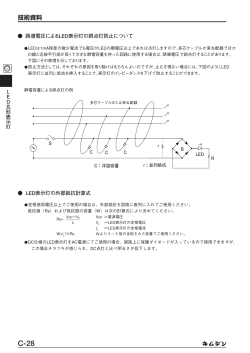
< IGBT MODULES >
CM300DY-24S
HIGH POWER SWITCHING USE
INSULATED TYPE
Collector current I C .............….......................…
300A
Collector-emitter voltage V CES ......................… 1 2 0 0 V
Maximum junction temperature T j m a x ..............
1 7 5 °C
●Flat base Type
●Copper base plate
●RoHS Directive compliance
●UL Recognized under UL1557, File E323585
Dual switch (Half-Bridge)
APPLICATION
AC Motor Control, Motion/Servo Control, Power supply, etc.
OUTLINE DRAWING & INTERNAL CONNECTION
Dimension in mm
INTERNAL CONNECTION
3
Tolerance
0.5
to
±0.2
over
3
to
6
±0.3
over
6
to
30
±0.5
over 30
to 120
±0.8
over 120
to 400
±1.2
Di1
C2E1
Tr2
E2
Di2
Publication Date : April 2013
1
Tr1
C1
G1 E1
(Es1)
Division of Dimension
E2 G2
(Es2)
Tolerance otherwise specified
< IGBT MODULES >
CM300DY-24S
HIGH POWER SWITCHING USE
INSULATED TYPE
ABSOLUTE MAXIMUM RATINGS (Tj=25 °C, unless otherwise specified)
Rating
Unit
VCES
Symbol
Collector-emitter voltage
G-E short-circuited
1200
V
VGES
Gate-emitter voltage
C-E short-circuited
± 20
V
IC
Item
Ptot
IE
IERM
(Note1)
TC=25 °C
300
(Note3)
Pulse, Repetitive
Total power dissipation
(Note1)
(Note2, 4)
DC, TC=119 °C
Collector current
ICRM
Conditions
(Note2, 4)
2270
(Note2)
Emitter current
A
600
W
300
Pulse, Repetitive
(Note3)
A
600
Visol
Isolation voltage
Terminals to base plate, RMS, f=60 Hz, AC 1 min
2500
Tjmax
Maximum junction temperature
Instantaneous event (overload)
175
V
Tcmax
Maximum case temperature
(Note4)
125
Tjopr
Operating junction temperature
Continuous operation (under switching)
-40 ~ +150
Tstg
Storage temperature
-
-40 ~ +125
°C
°C
ELECTRICAL CHARACTERISTICS (T j =25 °C, unless otherwise specified)
Symbol
Item
Limits
Conditions
Min.
Typ.
Max.
Unit
ICES
Collector-emitter cut-off current
VCE=VCES, G-E short-circuited
-
-
1.0
mA
IGES
Gate-emitter leakage current
VGE=VGES, C-E short-circuited
-
-
0.5
μA
VGE(th)
Gate-emitter threshold voltage
IC=30 mA, VCE=10 V
5.4
6.0
6.6
V
IC=300 A
VCEsat
Collector-emitter saturation voltage
Cies
Input capacitance
Coes
Output capacitance
Cres
Reverse transfer capacitance
QG
Gate charge
td(on)
Turn-on delay time
tr
Rise time
td(off)
Turn-off delay time
tf
Fall time
T j =25 °C
-
1.80
2.25
VGE=15 V,
T j =125 °C
-
2.00
-
Terminal
T j =150 °C
-
2.05
-
IC=300 A
(Note1)
Emitter-collector voltage
trr
(Note1)
Reverse recovery time
Qrr
(Note1)
(Note5)
,
T j =25 °C
-
1.70
2.15
VGE=15 V,
T j =125 °C
-
1.90
-
Chip
T j =150 °C
-
1.95
-
-
-
30
,
VCE=10 V, G-E short-circuited
VCC=600 V, IC=300 A, VGE=15 V
VCC=600 V, IC=300 A, VGE=±15 V,
RG=0 Ω, Inductive load
-
-
6.0
-
-
0.5
-
700
-
-
-
800
-
-
200
-
-
600
nF
nC
ns
-
-
300
1.80
2.25
G-E short-circuited,
T j =125 °C
-
1.80
-
Terminal
T j =150 °C
-
1.80
-
T j =25 °C
-
1.70
2.15
G-E short-circuited,
T j =125 °C
-
1.70
-
Chip
T j =150 °C
-
1.70
-
VCC=600 V, IE=300 A, VGE=±15 V,
-
-
300
ns
μC
IE=300 A
(Note5)
,
,
Reverse recovery charge
RG=0 Ω, Inductive load
-
16
-
Turn-on switching energy per pulse
VCC=600 V, IC=IE=300 A,
-
41
-
Eoff
Turn-off switching energy per pulse
VGE=±15 V, RG=0 Ω,
-
32
-
(Note1)
V
-
(Note5)
Eon
Err
V
T j =25 °C
IE=300 A
VEC
(Note5)
V
V
mJ
Reverse recovery energy per pulse
T j =150 °C, Inductive load
-
22
-
mJ
RCC'+EE'
Internal lead resistance
Main terminals -chip, per switch, T C =25 °C
-
-
0.9
mΩ
rg
Internal gate resistance
Per switch
-
6.5
-
Ω
Publication Date : April 2013
2
< IGBT MODULES >
CM300DY-24S
HIGH POWER SWITCHING USE
INSULATED TYPE
THERMAL RESISTANCE CHARACTERISTICS
Symbol
Rth(j-c)Q
Rth(j-c)D
Rth(c-s)
Item
Thermal resistance
(Note4)
Contact thermal resistance
Limits
Conditions
(Note4)
Min.
Typ.
Max.
Unit
Junction to case, per IGBT
-
-
66
K/kW
Junction to case, per FWDi
-
-
120
K/kW
-
20
-
K/kW
Case to heat sink, per 1/2 module,
Thermal grease applied
(Note6)
MECHANICAL CHARACTERISTICS
Symbol
Mt
Item
Mounting torque
Ms
Limits
Conditions
Min.
Typ.
Max.
Unit
Main terminals
M 6 screw
3.5
4.0
4.5
N·m
Mounting to heat sink
M 6 screw
3.5
4.0
4.5
N·m
-
400
-
g
-100
-
+100
μm
m
Weight
-
ec
Flatness of base plate
On the centerline X, Y
(Note7)
-: Concave
+: Convex
Note1. Represent ratings and characteristics of the anti-parallel, emitter-collector free wheeling diode (FWDi).
2. Junction temperature (T j ) should not increase beyond T j m a x rating.
3. Pulse width and repetition rate should be such that the device junction temperature (T j ) dose not exceed T j m a x rating.
4. Case temperature (TC) and heat sink temperature (T s ) are defined on the each surface (mounting side) of base plate and heat sink just under
the chips. Refer to the figure of chip location.
The heat sink thermal resistance should measure just under the chips.
5. Pulse width and repetition rate should be such as to cause negligible temperature rise. Refer to the figure of test circuit.
6. Typical value is measured by using thermally conductive grease of λ=0.9 W/(m·K).
7. Base plate (mounting side) flatness measurement points (X, Y) are as follows of the following figure.
X
Mounting side
3 mm
Y
Mounting side
-: Concave
Mounting side
+: Convex
RECOMMENDED OPERATING CONDITIONS
Symbol
VCC
Item
(DC) Supply voltage
Conditions
Applied across C1-E2
VGEon
Gate (-emitter drive) voltage
Applied across G1-Es1/G2-Es2
RG
External gate resistance
Per switch
Publication Date : April 2013
3
Limits
Unit
Min.
Typ.
Max.
-
600
850
13.5
15.0
16.5
V
0
-
14
Ω
V
< IGBT MODULES >
CM300DY-24S
HIGH POWER SWITCHING USE
INSULATED TYPE
CHIP LOCATION (Top view)
Dimension in mm, tolerance: ±1 mm
Tr1/Tr2: IGBT, Di1/Di2: FWDi
TEST CIRCUIT
C1
C1
VGE=15 V
IC
G1
V
Shortcircuited
G1
Shortcircuited
V
IC
G2
Tr1
C2E1
C2E1
VGE=15 V
Tr2
Di1
Di2
VEC test circuit
Publication Date : April 2013
4
E2
Es2
E2
Es2
V C E s a t test circuit
IE
G2
G2
E2
Es2
E2
Es2
V
Es1
Es1
Shortcircuited
VGE=15 V
G2
G1
V
C2E1
C2E1
IE
Shortcircuited
G1
Es1
Es1
C1
C1
Shortcircuited
< IGBT MODULES >
CM300DY-24S
HIGH POWER SWITCHING USE
INSULATED TYPE
TEST CIRCUIT AND WAVEFORMS
~
vGE
iE
C1
90 %
0V
G1
-VGE
0
iE
t
Load
Es1
VC C
IE
iC
~
~
+
C2E1
RG
G2
vG E
0V
-V GE
iC
0A
tr
t d( o n)
tf
t d ( o f f)
t
Switching characteristics test circuit and waveforms
t r r , Q r r test waveform
iE
vCE
0
iC
iC
VCC
0.1×ICM
0.1×VCC
ICM
VCC
t
0.5×I r r
10%
E2
ICM
t
Irr
vCE
Es2
trr
0A
90 %
+V GE
Q r r =0.5×I r r ×t r r
0
0.1×VCC
IEM
vEC
vCE
0.02×ICM
ti
ti
IGBT Turn-on switching energy
IGBT Turn-off switching energy
t
VCC
0A
t
0V
t
ti
FWDi Reverse recovery energy
Turn-on / Turn-off switching energy and Reverse recovery energy test waveforms (Integral time instruction drawing)
Publication Date : April 2013
5
< IGBT MODULES >
CM300DY-24S
HIGH POWER SWITCHING USE
INSULATED TYPE
PERFORMANCE CURVES
OUTPUT CHARACTERISTICS
(TYPICAL)
COLLECTOR-EMITTER SATURATION
VOLTAGE CHARACTERISTICS
(TYPICAL)
T j =25 °C
VGE=15 V
(Chip)
VGE=20 V
12 V
T j =125 °C
3
COLLECTOR-EMITTER
SATURATION VOLTAGE VCEsat (V)
IC (A)
COLLECTOR CURRENT
13.5 V
15 V
500
400
11 V
300
10 V
200
9V
100
T j =150 °C
2.5
2
T j =25 °C
1.5
1
0.5
0
0
0
2
4
6
8
COLLECTOR-EMITTER VOLTAGE
0
10
100
VCE (V)
T j =25 °C
200
300
400
COLLECTOR CURRENT
COLLECTOR-EMITTER SATURATION
VOLTAGE CHARACTERISTICS
(TYPICAL)
500
600
IC (A)
FREE WHEELING DIODE
FORWARD CHARACTERISTICS
(TYPICAL)
G-E short-circuited
(Chip)
(Chip)
1000
10
8
IC=600 A
IE (A)
T j =150 °C
IC=300 A
6
EMITTER CURRENT
COLLECTOR-EMITTER
SATURATION VOLTAGE VCEsat (V)
(Chip)
3.5
600
IC=120 A
4
T j =125 °C
100
T j =25 °C
2
0
10
6
8
10
12
14
GATE-EMITTER VOLTAGE
16
18
0
20
VGE (V)
0.5
1
1.5
2
EMITTER-COLLECTOR VOLTAGE
Publication Date : April 2013
6
2.5
VEC (V)
3
< IGBT MODULES >
CM300DY-24S
HIGH POWER SWITCHING USE
INSULATED TYPE
PERFORMANCE CURVES
HALF-BRIDGE
SWITCHING CHARACTERISTICS
(TYPICAL)
VCC=600 V, VGE=±15 V, RG=0 Ω, INDUCTIVE LOAD
---------------: T j =150 °C, - - - - -: T j =125 °C
HALF-BRIDGE
SWITCHING CHARACTERISTICS
(TYPICAL)
VCC=600 V, IC=300 A, VGE=±15 V, INDUCTIVE LOAD
---------------: T j =150 °C, - - - - -: T j =125 °C
1000
10000
1000
td(off)
td(off), tf
tr
td(on), tr
SWITCHING TIME
(ns)
tf
SWITCHING TIME
100
tr
10
1000
100
td(off)
tf
100
100
10
10
100
COLLECTOR CURRENT
1000
0.1
IC (A)
1
10
EXTERNAL GATE RESISTANCE
HALF-BRIDGE
SWITCHING CHARACTERISTICS
(TYPICAL)
VCC=600 V, VGE=±15 V, RG=0 Ω,
INDUCTIVE LOAD, PER PULSE
---------------: T j =150 °C, - - - - -: T j =125 °C
RG (Ω)
HALF-BRIDGE
SWITCHING CHARACTERISTICS
(TYPICAL)
VCC=600 V, IC/IE=300 A, VGE=±15 V,
INDUCTIVE LOAD, PER PULSE
---------------: T j =150 °C, - - - - -: T j =125 °C
100
100
SWITCHING ENERGY (mJ)
REVERSE RECOVERY ENERGY (mJ)
SWITCHING ENERGY (mJ)
REVERSE RECOVERY ENERGY (mJ)
Eon
Err
10
Eoff
Eon
1
Eoff
Err
10
1
10
100
1000
0.01
0.1
1
EXTERNAL GATE RESISTANCE
COLLECTOR CURRENT IC (A)
EMITTER CURRENT IE (A)
Publication Date : April 2013
7
10
RG (Ω)
100
SWITCHING TIME
td(on)
(ns)
(ns)
td(on)
< IGBT MODULES >
CM300DY-24S
HIGH POWER SWITCHING USE
INSULATED TYPE
PERFORMANCE CURVES
CAPACITANCE CHARACTERISTICS
(TYPICAL)
FREE WHEELING DIODE
REVERSE RECOVERY CHARACTERISTICS
(TYPICAL)
VCC=600 V, VGE=±15 V, RG=0 Ω, INDUCTIVE LOAD
---------------: T j =150 °C, - - - - -: T j =125 °C
G-E short-circuited, T j =25 °C
1000
100
Cies
trr
I r r (A), t r r (ns)
CAPACITANCE (nF)
10
Coes
1
Irr
100
Cres
0.1
0.01
10
0.1
1
10
COLLECTOR-EMITTER VOLTAGE
10
100
IE (A)
GATE CHARGE CHARACTERISTICS
(TYPICAL)
TRANSIENT THERMAL IMPEDANCE CHARACTERISTICS
(MAXIMUM)
V C C = 600 V, I C = 300 A, T j =25 °C
Single pulse, TC=25°C
R t h ( j - c ) Q =66 K/kW, R t h ( j - c ) D =120 K/kW
Zth(j-c)
NORMALIZED TRANSIENT THERMAL IMPEDANCE
VGE (V)
GATE-EMITTER VOLTAGE
1000
EMITTER CURRENT
20
15
10
5
0
0
100
VCE (V)
200
400
GATE CHARGE
600
800
1000
QG (nC)
1
0.1
0.01
0.001
0.00001
0.0001
0.001
0.01
TIME (S)
Publication Date : April 2013
8
0.1
1
10
< IGBT MODULES >
CM300DY-24S
HIGH POWER SWITCHING USE
INSULATED TYPE
Keep safety first in your circuit designs!
Mitsubishi Electric Corporation puts the maximum effort into making semiconductor products better and more
reliable, but there is always the possibility that trouble may occur with them. Trouble with semiconductors
may lead to personal injury, fire or property damage. Remember to give due consideration to safety when
making your circuit designs, with appropriate measures such as (i) placement of substitutive, auxiliary
circuits, (ii) use of non-flammable material or (iii) prevention against any malfunction or mishap.
Notes regarding these materials
•These materials are intended as a reference to assist our customers in the selection of the Mitsubishi
semiconductor product best suited to the customer's application; they do not convey any license under any
intellectual property rights, or any other rights, belonging to Mitsubishi Electric Corporation or a third party.
•Mitsubishi Electric Corporation assumes no responsibility for any damage, or infringement of any
third-party's rights, originating in the use of any product data, diagrams, charts, programs, algorithms, or
circuit application examples contained in these materials.
•All information contained in these materials, including product data, diagrams, charts, programs and
algorithms represents information on products at the time of publication of these materials, and are subject
to change by Mitsubishi Electric Corporation without notice due to product improvements or other reasons. It
is therefore recommended that customers contact Mitsubishi Electric Corporation or an authorized
Mitsubishi Semiconductor product distributor for the latest product information before purchasing a product
listed herein.
The information described here may contain technical inaccuracies or typographical errors. Mitsubishi
Electric Corporation assumes no responsibility for any damage, liability, or other loss rising from these
inaccuracies or errors.
Please also pay attention to information published by Mitsubishi Electric Corporation by various means,
including the Mitsubishi Semiconductor home page (www.MitsubishiElectric.com/semiconductors/).
•When using any or all of the information contained in these materials, including product data, diagrams,
charts, programs, and algorithms, please be sure to evaluate all information as a total system before making
a final decision on the applicability of the information and products. Mitsubishi Electric Corporation assumes
no responsibility for any damage, liability or other loss resulting from the information contained herein.
•Mitsubishi Electric Corporation semiconductors are not designed or manufactured for use in a device or
system that is used under circumstances in which human life is potentially at stake. Please contact
Mitsubishi Electric Corporation or an authorized Mitsubishi Semiconductor product distributor when
considering the use of a product contained herein for any specific purposes, such as apparatus or systems
for transportation, vehicular, medical, aerospace, nuclear, or undersea repeater use.
•The prior written approval of Mitsubishi Electric Corporation is necessary to reprint or reproduce in whole or
in part these materials.
•If these products or technologies are subject to the Japanese export control restrictions, they must be
exported under a license from the Japanese government and cannot be imported into a country other than
the approved destination.
Any diversion or reexport contrary to the export control laws and regulations of Japan and/or the country of
destination is prohibited.
•Please contact Mitsubishi Electric Corporation or an authorized Mitsubishi Semiconductor product distributor
for further details on these materials or the products contained therein.
© 2013 MITSUBISHI ELECTRIC CORPORATION. ALL RIGHTS RESERVED.
Publication Date : April 2013
9
<IGBT モジュール>
CM300DY-24S
大電力スイッチング用
絶縁形
コレクタ電流 IC .......................................
300A
コレクタ・エミッタ間電圧 VCES ............... 1 2 0 0 V
最大接合温度 Tjmax ............................... 1 7 5 °C
●フラットベース形
●銅ベース板
●RoHS 指令対応
●UL Recognized under UL1557, File E323585
2素子入
用途
インバータ装置,サーボアンプ,電源装置 など
外形及び接続図
単位:mm
E2 G2
(Es2)
接続図
Tolerance otherwise specified
Tolerance
0.5
to
3
±0.2
over
3
to
6
±0.3
over
6
to
30
±0.5
over 30
to 120
±0.8
over 120
to 400
±1.2
Di1
C2E1
Tr2
E2
Di2
2013年4月作成
1
Tr1
C1
G1 E1
(Es1)
Division of Dimension
<IGBT モジュール>
CM300DY-24S
大電力スイッチング用
絶縁形
絶対最大定格(指定のない場合,Tj=25 °C)
記号
項目
条件
定格値
単位
VCES
コレクタ・エミッタ間電圧
G-E 間短絡
1200
V
VGES
ゲート・エミッタ間電圧
C-E 間短絡
± 20
V
IC
コレクタ電流
ICRM
Ptot
パルス, 繰返し
TC=25 °C
コレクタ損失
IE
(注1)
IERM
(注1)
(注2, 4)
直流, TC=119 °C
300
(注3)
(注2,4)
2270
(注2)
エミッタ電流
A
600
W
300
パルス, 繰返し
(注3)
A
600
Visol
絶縁耐電圧
全端子・ベース板間, 実効値, f=60 Hz, AC 1 分間
2500
Tjmax
最大接合温度
瞬時動作(過負荷等)
175
V
Tcmax
最大ケース温度
(注4)
125
Tjopr
動作接合温度
連続動作
-40 ~ +150
Tstg
保存温度
-
-40 ~ +125
°C
°C
電気的特性(指定のない場合,T j =25 °C)
記号
項目
規格値
条件
最小
標準
最大
単位
ICES
コレクタ・エミッタ間遮断電流
VCE=VCES, G-E 間短絡
-
-
1.0
mA
IGES
ゲート・エミッタ間漏れ電流
VGE=VGES, C-E 間短絡
-
-
0.5
μA
VGE(th)
ゲート・エミッタ間しきい値電圧
IC=30 mA, VCE=10 V
5.4
6.0
6.6
V
IC=300 A
VCEsat
コレクタ・エミッタ間飽和電圧
Cies
入力容量
Coes
出力容量
Cres
帰還容量
QG
ゲート電荷量
td(on)
ターンオン遅れ時間
tr
上昇時間
td(off)
ターンオフ遅れ時間
tf
下降時間
(注5)
,
T j =25 °C
-
1.80
2.25
VGE=15 V
T j =125 °C
-
2.00
-
端子
T j =150 °C
-
2.05
-
IC=300 A
(注5)
,
T j =25 °C
-
1.70
2.15
VGE=15 V
T j =125 °C
-
1.90
-
チップ
T j =150 °C
-
1.95
-
-
-
30
-
-
6.0
-
-
0.5
-
700
-
-
-
800
VCE=10 V, G-E 間短絡
VCC=600 V, IC=300 A, VGE=15 V
VCC=600 V, IC=300 A, VGE=±15 V,
RG=0 Ω, 誘導負荷
エミッタ・コレクタ間電圧
200
600
-
-
300
-
1.80
2.25
T j =125 °C
-
1.80
-
T j =150 °C
-
1.80
-
T j =25 °C
-
1.70
2.15
G-E 間短絡,
T j =125 °C
-
1.70
-
端子
T j =150 °C
-
1.70
-
(注5)
,
G-E 間短絡,
(注1)
-
T j =25 °C
IE=300 A
VEC
-
端子
IE=300 A
(注5)
,
V
V
nF
nC
ns
V
V
trr
(注1)
逆回復時間
VCC=600 V, IE=300 A, VGE=±15 V,
-
-
300
ns
Qrr
(注1)
逆回復電荷
RG=0 Ω, 誘導負荷
-
16
-
μC
Eon
ターンオンスイッチング損失
VCC=600 V, IC=IE=300 A,
-
41
-
Eoff
ターンオフスイッチング損失
VGE=±15 V, RG=0 Ω, T j =150 °C,
-
32
-
Err
(注1)
mJ
逆回復損失
誘導負荷, 1 パルスあたり
-
22
-
mJ
RCC'+EE'
内部配線抵抗
主端子・チップ間, 1 素子あたり, T C =25 °C
-
-
0.9
mΩ
rg
内部ゲート抵抗
1 素子あたり
-
6.5
-
Ω
2013年4月作成
2
<IGBT モジュール>
CM300DY-24S
大電力スイッチング用
絶縁形
熱的特性
記号
項目
Rth(j-c)Q
熱抵抗
Rth(j-c)D
規格値
条件
(注2)
最大
単位
最小
標準
接合・ケース間, IGBT 1 素子あたり
-
-
66
K/kW
接合・ケース間, FWDi 1 素子あたり
-
-
120
K/kW
-
20
-
K/kW
ケース・ヒートシンク間,
Rth(c-s)
接触熱抵抗
1/2 モジュールあたり,
(注2)
熱伝導性グリース塗布
(注6)
機械的定格及び特性
記号
項目
Mt
締付けトルク
Ms
規格値
条件
最小
標準
最大
単位
主端子
M 6 ネジ
3.5
4.0
4.5
N·m
取付け
M 6 ネジ
3.5
4.0
4.5
N·m
-
400
-
g
-100
-
+100
μm
m
質量
-
ec
ベース板平面度
X, Y 各中心線上
(注7)
-: 凹
+: 凸
注 1. フリーホイールダイオード(FWDi)の定格又は特性を示します。
2. ケース温度(T C )及びヒートシンク温度(T s )の定義点は,チップ直下におけるベース板及びヒートシンクの表面です。
チップ中心位置は,チップ配置図のとおりです。
3. パルス幅及び繰返し率は,素子の温度上昇が,最大接合温度(T j m a x =150 °C)を越えない値とします。
4. 接合温度は,最大接合温度(T j m a x =150 °C)以下です。
5. パルス幅及び繰返し率は,素子の温度上昇が無視できる値とします。
(試験回路は,「V C E s a t 」「VEC」試験回路図を参照)
6. 接触熱抵抗の標準値は,熱伝導率 λ=0.9 W/(m·K) の放熱用グリースを使用したときの値です。
7. ベース板(取付面)平面度測定箇所は,下図のとおりです。
取付面
X
3 mm
Y
取付面
-: 凹
取付面
+: 凸
推奨動作条件
記号
項目
条件
VCC
電源電圧
C1-E2 端子間
VGEon
ゲート(駆動)電圧
G1-Es1/G2-Es2 端子間
RG
外部ゲート抵抗
1 素子あたり
2013年4月作成
3
規格値
最小
標準
最大
-
600
850
13.5
15.0
16.5
0
-
14
Unit
V
Ω
<IGBT モジュール>
CM300DY-24S
大電力スイッチング用
絶縁形
チップ配置図 (Top view)
単位:mm, 公差:±1 mm
Tr1/Tr2: IGBT, Di1/Di2: FWDi。記号は,それぞれのチップの中心を示します。
試験回路
C1
C1
VGE=15 V
IC
G1
V
Shortcircuited
G1
Shortcircuited
V
IC
G2
E2
Es2
Tr1
C2E1
C2E1
VGE=15 V
Tr2
Di1
Di2
VEC 特性試験回路
2013年4月作成
4
E2
Es2
E2
Es2
V C E s a t 特性試験回路
IE
G2
G2
E2
Es2
V
Es1
Es1
Shortcircuited
VGE=15 V
G2
G1
V
C2E1
C2E1
IE
Shortcircuited
G1
Es1
Es1
C1
C1
Shortcircuited
<IGBT モジュール>
CM300DY-24S
大電力スイッチング用
絶縁形
試験回路及び試験波形
~
vGE
iE
C1
90 %
0V
G1
-VGE
0
iE
t
Load
Es1
VC C
IE
iC
~
~
+
C2E1
RG
G2
vG E
0V
-V GE
iC
0A
tr
t d( o n)
tf
t d ( o f f)
t
スイッチング特性試験回路及び試験波形
逆回復特性試験波形
iE
vCE
0
iC
iC
VCC
0.1×ICM
0.1×VCC
ICM
VCC
t
0.5×I r r
10%
E2
ICM
t
Irr
vCE
Es2
trr
0A
90 %
+V GE
Q r r =0.5×I r r ×t r r
0
0.1×VCC
IEM
vEC
vCE
0.02×ICM
t
ti
ti
IGBT ターンオンスイッチング損失
IGBT ターンオフスイッチング損失
0A
t
0V
t
ti
FWDi 逆回復損失
ターンオン / ターンオフスイッチング損失及び逆回復損失試験波形(積分時間説明図)
2013年4月作成
5
VCC
<IGBT モジュール>
CM300DY-24S
大電力スイッチング用
絶縁形
特性図
出力特性
(代表例)
コレクタ・エミッタ間飽和電圧特性
(代表例)
T j =25 °C
VGE=15 V
(チップ)
600
(チップ)
3.5
13.5 V
VGE=20 V
12 V
VCEsat
400
コレクタ・エミッタ間飽和電圧
11 V
コレクタ電流
IC
(A)
(V)
15 V
500
300
10 V
200
9V
100
0
T j =125 °C
3
T j =150 °C
2.5
2
T j =25 °C
1.5
1
0.5
0
0
2
4
6
コレクタ・エミッタ間電圧
8
VCE
0
10
100
T j =25 °C
400
IC
500
600
(A)
フリーホイールダイオード順特性
(代表例)
G-E間短絡
(チップ)
(チップ)
1000
10
8
IC=600 A
VCEsat
T j =150 °C
(A)
IC=300 A
IE
6
IC=120 A
エミッタ電流
(V)
300
コレクタ電流
コレクタ・エミッタ間飽和電圧特性
(代表例)
コレクタ・エミッタ間飽和電圧
200
(V)
4
T j =125 °C
100
T j =25 °C
2
0
10
6
8
10
12
14
ゲート・エミッタ間電圧
16
18
0
20
VGE (V)
0.5
1
1.5
エミッタ・コレクタ間電圧
2013年4月作成
6
2
VEC
2.5
(V)
3
<IGBT モジュール>
CM300DY-24S
大電力スイッチング用
絶縁形
特性図
スイッチング時間特性
(代表例)
スイッチング時間特性
(代表例)
VCC=600 V, VGE=±15 V, RG=0 Ω, 誘導負荷
---------------: T j =150 °C, - - - - -: T j =125 °C
VCC=600 V, IC=300 A, VGE=±15 V, 誘導負荷
---------------: T j =150 °C, - - - - -: T j =125 °C
1000
10000
1000
td(off)
tr
100
100
1000
スイッチング時間
スイッチング時間
tr, tf
td(off), tf
tf
(ns)
スイッチング時間
(ns)
td(on)
(ns)
td(on)
td(off)
tr
tf
10
10
10
100
コレクタ電流
1000
IC
0.1
(A)
1
外部ゲート抵抗
スイッチング損失特性
(代表例)
VCC=600 V, VGE=±15 V, RG=0 Ω,
誘導負荷, 1パルスあたり
---------------: T j =150 °C, - - - - -: T j =125 °C
100
100
10
RG
(Ω)
スイッチング損失特性
(代表例)
VCC=600 V, IC/IE=300 A, VGE=±15 V,
誘導負荷, 1パルスあたり
---------------: T j =150 °C, - - - - -: T j =125 °C
100
Eon
10
Eoff
Eon
1
(mJ)
スイッチング損失, 逆回復損失
(mJ)
スイッチング損失 Eo f f
Err
スイッチング損失 Eo n
(mJ), 逆回復損失
(mJ)
100
Eoff
Err
10
1
10
100
コレクタ電流
エミッタ電流
1000
0.01
IC (A)
IE (A)
0.1
1
外部ゲート抵抗
2013年4月作成
7
10
RG
(Ω)
100
<IGBT モジュール>
CM300DY-24S
大電力スイッチング用
絶縁形
特性図
容量特性
(代表例)
フリーホイールダイオード逆回復特性
(代表例)
G-E間短絡, T j =25 °C
VCC=600 V, VGE=±15 V, RG=0 Ω, 誘導負荷
---------------: T j =150 °C, - - - - -: T j =125 °C
1000
100
Cies
trr
Irr
(A)
Coes
100
trr
Irr
容量
1
(ns)
(nF)
10
Cres
0.1
0.01
10
0.1
1
10
コレクタ・エミッタ間電圧
VCE
10
100
100
(V)
エミッタ電流
ゲート容量特性
(代表例)
Single pulse, TC=25°C
R t h ( j - c ) Q =66 K/kW, R t h ( j - c ) D =120 K/kW
Zth(j-c)
NORMALIZED TRANSIENT THERMAL IMPEDANCE
ゲート・エミッタ間電圧
VGE (V)
20
15
10
5
0
200
400
ゲート容量
600
QG
(A)
最大過渡熱インピーダンス特性
V C C = 600 V, I C = 300 A, T j =25 °C
0
1000
IE
800
1000
(nC)
1
0.1
0.01
0.001
0.00001
0.0001
0.001
0.01
時間
2013年4月作成
8
(S)
0.1
1
10
<IGBT モジュール>
CM300DY-24S
大電力スイッチング用
絶縁形
安全設計に関するお願い
弊 社 は 品 質 ,信 頼 性 の 向 上 に 努 め て お り ま す が ,半 導 体 製 品 は 故 障 が 発 生 し た り ,誤 動 作 す る 場 合 が あ り
ま す 。弊 社 の 半 導 体 製 品 の 故 障 又 は 誤 動 作 に よ っ て 結 果 と し て ,人 身 事 故 ,火 災 事 故 、社 会 的 損 害 な ど を 生
じ さ せ な い よ う な 安 全 性 を 考 慮 し た 冗 長 設 計 ,延 焼 対 策 設 計 ,誤 動 作 防 止 設 計 な ど の 安 全 設 計 に 十 分 ご 留 意
ください。
本資料ご利用に際しての留意事項
・本 資 料 は ,お 客 様 が 用 途 に 応 じ た 適 切 な 三 菱 半 導 体 製 品 を ご 購 入 い た だ く た め の 参 考 資 料 で あ り ,本 資 料
中 に 記 載 の 技 術 情 報 に つ い て 三 菱 電 機 が 所 有 す る 知 的 財 産 権 そ の 他 の 権 利 の 実 施 、使 用 を 許 諾 す る も の で
はありません。
・本 資 料 に 記 載 の 製 品 デ ー タ ,図 ,表 ,プ ロ グ ラ ム ,ア ル ゴ リ ズ ム そ の 他 応 用 回 路 例 の 使 用 に 起 因 す る 損 害 、
第三者所有の権利に対する侵害に関し、三菱電機は責任を負いません。
・ 本 資 料 に 記 載 の 製 品 デ ー タ ,図 ,表 ,プ ロ グ ラ ム ,ア ル ゴ リ ズ ム そ の 他 全 て の 情 報 は 本 資 料 発 行 時 点 の も
の で あ り ,三 菱 電 機 は ,予 告 な し に ,本 資 料 に 記 載 し た 製 品 又 は 仕 様 を 変 更 す る こ と が あ り ま す 。三 菱 半
導 体 製 品 の ご 購 入 に 当 た り ま し て は ,事 前 に 三 菱 電 機 ま た は 特 約 店 へ 最 新 の 情 報 を ご 確 認 頂 き ま す と と も
に 、三 菱 電 機 半 導 体 情 報 ホ ー ム ペ ー ジ( www.MitsubishiElectric.co.jp/semiconductors/)な ど を 通 じ て 公 開
される情報に常にご注意ください。
・本 資 料 に 記 載 し た 情 報 は 、正 確 を 期 す た め 、慎 重 に 制 作 し た も の で す が 、万 一 本 資 料 の 記 述 誤 り に 起 因 す
る損害がお客様に生じた場合には、三菱電機はその責任を負いません。
・本 資 料 に 記 載 の 製 品 デ ー タ 、図 、表 に 示 す 技 術 的 な 内 容 、プ ロ グ ラ ム 及 び ア ル ゴ リ ズ ム を 流 用 す る 場 合 は 、
技 術 内 容 、プ ロ グ ラ ム 、ア ル ゴ リ ズ ム 単 位 で 評 価 す る だ け で な く 、シ ス テ ム 全 体 で 十 分 に 評 価 し 、お 客 様
の責任において適用可否を判断してください。三菱電機は、適用可否に対する責任は負いません。
・本 資 料 に 記 載 さ れ た 製 品 は 、人 命 に か か わ る よ う な 状 況 の 下 で 使 用 さ れ る 機 器 あ る い は シ ス テ ム に 用 い ら
れ る こ と を 目 的 と し て 設 計 、製 造 さ れ た も の で は あ り ま せ ん 。本 資 料 に 記 載 の 製 品 を 運 輸 、移 動 体 用 、医
療 用 、航 空 宇 宙 用 、原 子 力 制 御 用 、海 底 中 継 用 機 器 あ る い は シ ス テ ム な ど 、特 殊 用 途 へ の ご 利 用 を ご 検 討
の際には、三菱電機または特約店へご照会ください。
・本資料の転載、複製については、文書による三菱電機の事前の承諾が必要です。
・本 資 料 に 関 し 詳 細 に つ い て の お 問 い 合 わ せ 、そ の 他 お 気 付 き の 点 が ご ざ い ま し た ら 三 菱 電 機 ま た は 特 約 店
までご照会ください。
© 2013 MITSUBISHI ELECTRIC CORPORATION. ALL RIGHTS RESERVED
2013年4月作成
9
© Copyright 2026 Paperzz