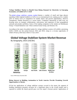
SGM9113
8MHz, 5th-Order Video Driver
with 6dB Gain
GENERAL DESCRIPTION
FEATURES
The SGM9113 is a single rail-to-rail 5th-order output
Excellent Video Performance
reconstruction filter with a -3dB bandwidth of 8MHz
5th-Order Reconstruction Filter
and 35V/µs slew rate. Operating from single power
Internal Gain: 6dB
supply ranging from 3.0V to 5.5V and sinking an
Rail-to-Rail Output
ultra-low 6mA quiescent current, the SGM9113 is
Input Voltage Range Includes Ground
ideally
Operates from 3.0V to 5.5V Single Power Supply
suited
for
low
power,
battery-operated
Low Power
applications.
6mA Typical Supply Current
The SGM9113 employs an internal level shift circuit
that
avoids
sync-pulse
clipping
and
allows
Available in Green SOIC-8 and SC70-5 Packages
-40℃ to +85℃ Operating Temperature Range
DC-coupled output. It operates over an ambient
temperature range of -40℃ to +85℃.
APPLICATIONS
Video Amplifiers
BLOCK DIAGRAM
Cable and Satellite Set-Top Boxes
Communication Devices
IN
6dB
Transparent Clamp
8MHz, 5th-Order
OUT
Video on Demand
Portable and Handheld Products
Personal Video Recorders
DVD Players
HDTV
SG Micro Corp
www.sg-micro.com
REV. A. 4
8MHz, 5th-Order Video Driver
with 6dB Gain
SGM9113
PACKAGE/ORDERING INFORMATION
MODEL
PACKAGE
DESCRIPTION
SPECIFIED
TEMPERATURE
RANGE
ORDERING
NUMBER
PACKAGE
MARKING
PACKING
OPTION
SOIC-8
-40℃ to +85℃
SGM9113YS8G/TR
SGM9113YS8
XXXXX
Tape and Reel, 2500
SC70-5
-40℃ to +85℃
SGM9113YC5G/TR
S23XX
Tape and Reel, 3000
SGM9113
NOTE: XX = Date Code. XXXXX = Date Code and Vendor
Code.
MARKING INFORMATION
S23 X X
Green (RoHS & HSF): SG Micro Corp defines "Green" to
mean Pb-Free (RoHS compatible) and free of halogen
substances. If you have additional comments or questions,
please contact your SGMICRO representative directly.
For example: S23FA (2015, January)
ABSOLUTE MAXIMUM RATINGS
ESD SENSITIVITY CAUTION
Input Voltage Range ..................... GND - 0.3V to VCC + 0.3V
Supply Voltage, VCC ....................................................... 6.0V
Junction Temperature .................................................. 150℃
Storage Temperature Range........................ -65℃ to +150℃
Lead Temperature (Soldering, 10s).............................. 260℃
ESD Susceptibility
HBM............................................................................ 8000V
MM................................................................................ 400V
CDM ........................................................................... 2000V
This integrated circuit can be damaged by ESD if you don’t
pay attention to ESD protection. SGMICRO recommends that
all integrated circuits be handled with appropriate precautions.
Failure to observe proper handling and installation
procedures can cause damage. ESD damage can range from
subtle performance degradation to complete device failure.
Precision integrated circuits may be more susceptible to
damage because very small parametric changes could cause
the device not to meet its published specifications.
RECOMMENDED OPERATING CONDITIONS
DISCLAIMER
Operating Voltage Range................................... 3.0V to 5.5V
Operating Temperature Range ...................... -40℃ to +85℃
SG Micro Corp reserves the right to make any change in
circuit design, specification or other related things if
necessary without notice at any time.
Date code - Month ("A" = Jan. "B" = Feb. … "L" = Dec.)
Date code - Year ("A" = 2010, "B" = 2011 …)
Chip I.D.
OVERSTRESS CAUTION
Stresses beyond those listed may cause permanent damage
to the device. Functional operation of the device at these or
any other conditions beyond those indicated in the
operational section of the specification is not implied.
Exposure to absolute maximum rating conditions for
extended periods may affect reliability.
SG Micro Corp
www.sg-micro.com
2
8MHz, 5th-Order Video Driver
with 6dB Gain
SGM9113
PIN CONFIGURATIONS
(TOP VIEW)
(TOP VIEW)
IN
1
NC
8
7
2
NC
VCC
3
6
4
5
OUT
IN
1
GND
2
VCC
3
5
OUT
4
GND
NC
NC
GND
NC = NO CONNECT
SC70-5
SOIC-8
PIN DESCRIPTION
PIN
NAME
FUNCTION
SOIC-8
SC70-5
1
1
IN
5
2, 4
GND
Ground.
4
3
VCC
Power Supply.
8
5
OUT
Signal Output.
2, 3, 6, 7
—
NC
SG Micro Corp
www.sg-micro.com
Signal Input.
No Connect.
3
8MHz, 5th-Order Video Driver
with 6dB Gain
SGM9113
ELECTRICAL CHARACTERISTICS
(At VCC = 5V, RL = 150Ω connected to GND, VIN = 1VPP and CIN = 0.1μF, output AC-coupled, referenced to 400kHz, unless
otherwise noted.)
PARAMETER
CONDITIONS
TEMP
MIN
TYP
MAX
340
570
UNITS
INPUT CHARACTERISTICS
Output Level Shift Voltage (VOLS)
VIN = 0V, No load
+25℃
675
-40℃ to +85℃
Input Voltage Clamp (VCLAMP)
Clamp Charge Current
Clamp Discharge Current
IIN = -3.5mA
VIN = VCLAMP - 100mV
VIN = 500mV
+25℃
-285
-40℃ to +85℃
-390
+25℃
-5.5
-40℃ to +85℃
-6.8
-210
RL = 150Ω
mA
2.7
3.2
-40℃ to +85℃
Voltage Gain (AV)
mV
-4.8
1.9
+25℃
+25℃
5.6
-40℃ to +85℃
5.55
+25℃
4.6
-40℃ to +85℃
4.5
+25℃
80
-40℃ to +85℃
77
6
mV
6.4
6.45
µA
dB
OUTPUT CHARACTERISTICS
Output Voltage High Swing
VIN = 3.0V, RL = 150Ω to GND
VIN = 1.5V, Out shorted to GND through
10Ω
Output Short-Circuit Current (ISC)
VIN = 0.5V, Out shorted to VCC through
10Ω
4.79
95
-102
+25℃
V
mA
-87
-78
-40℃ to +85℃
mA
POWER SUPPLY
Operating Voltage Range (VCC)
Power Supply Rejection Ratio (PSRR)
Quiescent Current (IQ)
VCC = 3.5V to 5.0V
VIN = 0.5V
+25℃
3.0
+25℃
40
-40℃ to +85℃
38
+25℃
5.5
50
6
dB
9.5
11.5
-40℃ to +85℃
V
mA
DYNAMIC PERFORMANCE
-0.1dB Bandwidth
+25℃
6
MHz
-3dB Bandwidth
+25℃
8
MHz
Filter Response (Normalized Gain)
fIN = 27MHz
+25℃
47
dB
Slew Rate
2V Output step, 80% to 20%
+25℃
35
V/µs
PAL DC-coupled
+25℃
0.85
%
PAL AC-coupled
+25℃
0.85
%
PAL DC-coupled
+25℃
1
°
PAL AC-coupled
+25℃
1.4
°
Group Delay Variation (D/DT)
Difference between 400kHz and 6.5MHz
+25℃
28
ns
Fall Time
2V Output step, 80% to 20%
+25℃
34
ns
Rise Time
2V Output step, 80% to 20%
+25℃
33
ns
Differential Gain Error (DG)
Differential Phase Error (DP)
SG Micro Corp
www.sg-micro.com
4
8MHz, 5th-Order Video Driver
with 6dB Gain
SGM9113
TYPICAL PERFORMANCE CHARACTERISTICS
At VCC = 5V, TA = +25℃, RL = 150Ω, output AC-coupled, unless otherwise noted.
Phase vs. Frequency
270
0
180
-3
90
Phase (degree)
Normalized Gain (dB)
Gain vs. Frequency
3
-6
-9
0
-90
-180
-12
-270
-15
0.1
1
10
Frequency (MHz)
0.1
100
1.20
0.12
0.60
0.00
-0.60
0.06
0.00
-0.06
-1.20
-0.12
-1.80
-0.25
-0.18
-0.25
0.55
0.75
Group Delay vs. Frequency
-0.05
0.15
0.35
Time (μs)
0.55
0.75
Gain Error vs. Temperature
0.12
100
0.1
Gain Error (%)
60
Group Delay (ns)
100
Small Signal Step Response
0.18
Output Voltage (V)
Output Voltage (V)
Large Signal Step Response
0.15
0.35
Time (µs)
10
Frequency (MHz)
1.80
-0.05
1
20
-20
-60
0.08
0.06
0.04
0.02
0
-100
0.1
1
10
Frequency (MHz)
SG Micro Corp
www.sg-micro.com
100
-40
-15
10
35
60
85
Temperature (℃)
5
8MHz, 5th-Order Video Driver
with 6dB Gain
SGM9113
TYPICAL PERFORMANCE CHARACTERISTICS
At VCC = 5V, TA = +25℃, RL = 150Ω, output AC-coupled, unless otherwise noted.
Quiescent Current vs. Supply Voltage
7
8
6.5
Quiescent Current (mA)
Quiescent Current (mA)
Quiescent Current vs. Temperature
10
6
4
2
5.5
5
-40
-15
10
35
60
85
Temperature (℃)
3
4
4.5
Supply Voltage (V)
Output Voltage Swing to the Positive Rail vs.
Output Current
Output Voltage Swing to the Negative Rail vs.
Output Current
5
3.5
5
5.5
1.4
1.2
Output Voltage (V)
4.8
Output Voltage (V)
6
4.6
+85℃
4.4
+25℃
-40℃
1
0.8
+85℃
+25℃
-40℃
0.6
0.4
4.2
0.2
4
0
0
20
40
60
Output Current (mA)
SG Micro Corp
www.sg-micro.com
80
100
0
20
40
60
Output Current (mA)
80
100
6
8MHz, 5th-Order Video Driver
with 6dB Gain
SGM9113
TYPICAL APPLICATION CIRCUITS
0.1µF
or 0.01µF
+5V
10µF
VCC
0.1µF
CVBS
IN
SGM9113
OUT
75Ω
75Ω 220µF
CVBS
GND
Figure 1. AC Coupling Application Schematic
0.1µF
or 0.01µF
+5V
10µF
VCC
0.1µF
CVBS
IN
SGM9113
OUT
75Ω
GND
75Ω 220µF
CVBS to Loading 1
CVBS to Loading 2
75Ω 220µF
Figure 2. Two Loading Output AC Coupling Application Schematic
NOTE:
1. Power supply VCC must be sequenced on first before input video signals.
SG Micro Corp
www.sg-micro.com
7
SGM9113
8MHz, 5th-Order Video Driver
with 6dB Gain
APPLICATION INFORMATION
Functional Description
Output Considerations
SGM9113 operates from a single 3.0V to 5.5V supply.
In application, SGM9113 is a fully integrated solution
for filtering and buffering SDTV signals in front of video
decoder or behind video encoder. For example,
SGM9113 can replace a passive LC filter and an
amplifier driver at CVBS side in set-top box and DVD
player. This solution can help reduce PCB size and
production cost, and it also improves video signal
performance comparing with traditional design using
discrete components. SGM9113 features a DC-coupled
input buffer, a 5-pole low-pass filter to eliminate out-ofband noise of video encoder, and a gain of 6dB in the
output amplifier to drive 75Ω load. The AC- or
DC-coupled input buffer eliminates sync crush, droop,
and field tilt. The output of SGM9113 also can be
DC-coupled or AC-coupled.
The SGM9113 outputs can be DC-coupled or
AC-coupled. When input is 0V, the SGM9113 output
voltage is 340mV typically. In DC coupling design, one
75Ω resistor is used to connect SGM9113’s output pin
with external load directly, and this serial back-termination
resistor is used to match the impedance of the
transmission line between SGM9113 and external load
to cancel the signal reflection. The SGM9113 outputs
can sink and source current allowing the device to be
AC-coupled with external load. In AC coupling, at least
220µF capacitor will be used in order to eliminate field
tilt.
The 85mA output current driving capability of the
SGM9113 is designed to drive two video lines
simultaneously - essentially a 75Ω load, while keeping
the output dynamic range as wide as possible.
Input Considerations
Besides AC coupling, the SGM9113 inputs also can be
DC-coupled. In DC coupling application, no input
coupling capacitors are needed because the amplitude
of input video signal from DAC includes ground and
extends up to 1.4V, and SGM9113 can be directly
connected to the output of a single-supply,
current-output DAC without any external bias network.
In applications where DAC’s output level exceeds the
range from 0V to 1.4V, or SGM9113 is driven by an
unknown external source or a SCART switch which has
its own clamping circuit, AC coupling is needed.
SG Micro Corp
www.sg-micro.com
Power-Supply Bypassing and Layout
Correct power supply bypassing is very important for
optimizing video performance in design. One 0.1µF and
one 10µF capacitors are always used to bypass VCC pin
of SGM9113. Place these two capacitors as close to
the SGM9113 supply pin as possible. A large ground
plane is also needed to ensure optimum performance.
The input and output termination resistors should be
placed as close to the related pins of SGM9113 as
possible to avoid performance degradation. The PCB
traces at the output side should have 75Ω characteristic
impedance in order to match the 75Ω characteristic
impedance of the cable connecting external load. In
design, keep the board trace at the inputs and outputs
of the SGM9113 as short as possible to minimize the
parasitic stray capacitance and noise pickup.
8
PACKAGE INFORMATION
PACKAGE OUTLINE DIMENSIONS
SOIC-8
0.6
D
e
2.2
E1
E
5.2
b
1.27
RECOMMENDED LAND PATTERN (Unit: mm)
L
A
A1
θ
c
A2
Symbol
Dimensions
In Millimeters
MIN
MAX
Dimensions
In Inches
MIN
MAX
A
1.350
1.750
0.053
0.069
A1
0.100
0.250
0.004
0.010
A2
1.350
1.550
0.053
0.061
b
0.330
0.510
0.013
0.020
c
0.170
0.250
0.006
0.010
D
4.700
5.100
0.185
0.200
E
3.800
4.000
0.150
0.157
E1
5.800
6.200
0.228
0.244
e
1.27 BSC
0.050 BSC
L
0.400
1.270
0.016
0.050
θ
0°
8°
0°
8°
SG Micro Corp
www.sg-micro.com
TX00010.000
PACKAGE INFORMATION
PACKAGE OUTLINE DIMENSIONS
SC70-5
D
e1
0.65
e
E1
1.9
E
0.75
b
0.4
1.3
RECOMMENDED LAND PATTERN (Unit: mm)
L
L1
A
θ
A1
A2
c
0.20
Symbol
Dimensions
In Millimeters
MIN
MAX
Dimensions
In Inches
MIN
MAX
A
0.900
1.100
0.035
0.043
A1
0.000
0.100
0.000
0.004
A2
0.900
1.000
0.035
0.039
b
0.150
0.350
0.006
0.014
c
0.080
0.150
0.003
0.006
D
2.000
2.200
0.079
0.087
E
1.150
1.350
0.045
0.053
E1
2.150
2.450
0.085
0.096
e
0.65 TYP
0.026 TYP
e1
1.300 BSC
0.051 BSC
L
0.525 REF
0.021 REF
L1
0.260
0.460
0.010
0.018
θ
0°
8°
0°
8°
SG Micro Corp
www.sg-micro.com
TX00043.000
PACKAGE INFORMATION
TAPE AND REEL INFORMATION
REEL DIMENSIONS
TAPE DIMENSIONS
P2
W
P0
Q1
Q2
Q1
Q2
Q1
Q2
Q3
Q4
Q3
Q4
Q3
Q4
B0
Reel Diameter
P1
A0
K0
Reel Width (W1)
DIRECTION OF FEED
NOTE: The picture is only for reference. Please make the object as the standard.
KEY PARAMETER LIST OF TAPE AND REEL
Reel
Diameter
Reel Width
W1
(mm)
A0
(mm)
B0
(mm)
K0
(mm)
P0
(mm)
P1
(mm)
P2
(mm)
W
(mm)
Pin1
Quadrant
SOIC-8
13″
12.4
6.4
5.4
2.1
4.0
8.0
2.0
12.0
Q1
SC70-5
7″
9.5
2.25
2.55
1.20
4.0
4.0
2.0
8.0
Q3
SG Micro Corp
www.sg-micro.com
DD0001
Package Type
TX10000.000
PACKAGE INFORMATION
CARTON BOX DIMENSIONS
NOTE: The picture is only for reference. Please make the object as the standard.
KEY PARAMETER LIST OF CARTON BOX
Length
(mm)
Width
(mm)
Height
(mm)
Pizza/Carton
7″ (Option)
368
227
224
8
7″
442
410
224
18
13″
386
280
370
5
SG Micro Corp
www.sg-micro.com
DD0002
Reel Type
TX20000.000
© Copyright 2026 Paperzz