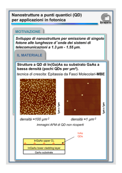
GaAs pillar array-based light emitting diodes fabricated by metal-assisted
chemical etching
Parsian K. Mohseni, Seung Hyun Kim, Xiang Zhao, Karthik Balasundaram, Jeong Dong Kim et al.
Citation: J. Appl. Phys. 114, 064909 (2013); doi: 10.1063/1.4817424
View online: http://dx.doi.org/10.1063/1.4817424
View Table of Contents: http://jap.aip.org/resource/1/JAPIAU/v114/i6
Published by the AIP Publishing LLC.
Additional information on J. Appl. Phys.
Journal Homepage: http://jap.aip.org/
Journal Information: http://jap.aip.org/about/about_the_journal
Top downloads: http://jap.aip.org/features/most_downloaded
Information for Authors: http://jap.aip.org/authors
Downloaded 29 Aug 2013 to 130.126.255.47. This article is copyrighted as indicated in the abstract. Reuse of AIP content is subject to the terms at: http://jap.aip.org/about/rights_and_permissions
JOURNAL OF APPLIED PHYSICS 114, 064909 (2013)
GaAs pillar array-based light emitting diodes fabricated by metal-assisted
chemical etching
Parsian K. Mohseni, Seung Hyun Kim, Xiang Zhao, Karthik Balasundaram,
Jeong Dong Kim, Lei Pan, John A. Rogers, James J. Coleman, and Xiuling Lia)
Departments of Electrical and Computer Engineering and Materials Science and Engineering, Micro and
Nanotechnology Laboratory, University of Illinois at Urbana-Champaign, Urbana, Illinois 61801, USA
(Received 23 May 2013; accepted 18 July 2013; published online 13 August 2013)
We demonstrate GaAs pillar array-based light emitting diodes (LEDs) with axial p-i-n junctions
fabricated using a room-temperature metal-assisted chemical etching (MacEtch) method.
Variations in vertical etch rates for all three doping types of GaAs are investigated as a function
of etching temperature, oxidant/acid concentration ratio, and dilution of the etching solution.
Control over nanopillar morphologies is demonstrated, simply through modification of the
etching conditions. Optical emission enhancement from the MacEtched p-i-n GaAs nanopillar
LED is observed, relative to the non-etched planar counterpart, through room-temperature
C 2013 AIP Publishing LLC.
photoluminescence and electroluminescence characterization. V
[http://dx.doi.org/10.1063/1.4817424]
I. INTRODUCTION
The metal-assisted chemical etching (MacEtch) method
for localized material removal from semiconductor surfaces,
as first established in the year 2000,1 allows for the formation
of high aspect-ratio nanostructures,2–4 deep vertical pits,5,6
and porous nano-membranes.7,8 Potential device applications
in photonics,9,10 optoelectronics,11 bio-sensing,12,13 energy
conversion,14–16 and energy storage17 have been envisioned.
However, the current state of research in this field is such
that focus is primarily placed upon the etching of Si,18 Ge,19
and semiconductor heterostructures composed thereof.20,21
To date, only few studies have been published in which
MacEtch of high aspect-ratio compound III–V semiconductors has been explored.22 Furthermore, systematic investigations regarding neither the role of dopant impurities nor the
influence of low- to room-temperature MacEtch of high
aspect-ratio GaAs structures have yet been established for
fabricating device structures.
The MacEtch mechanism relies, principally, on the
satisfaction of two conditions: (1) partial coverage of a semiconductor material by a layer composed of a noble metal
(typically, Au, Ag, or Pt), which acts as a catalyst for the
injection of holes (hþ) and, thereby, oxidation of the semiconductor directly below the interface and (2) submerging of
the metal-coated semiconductor into an etching solution containing an oxidant, which may accommodate hþ-injection
through the metal/semiconductor interface by way of a
reduction reaction, and an acid, capable of dissolving the
oxidized semiconductor where it is interfaced with the metallic catalyst layer.18,23 The continual repetition of such an oxidation and material dissolving cycle allows for anisotropic
etching of the semiconductor material, forcing the metal
layer to sink into the semiconductor.18,23
a)
Author to whom correspondence should be addressed. E-mail:
[email protected]
0021-8979/2013/114(6)/064909/6/$30.00
In comparison to other means of semiconductor
nanopillar array fabrication, MacEtch offers several key
advantages. The need for hazardous gases, a high thermal
budget, and high vacuum conditions are avoided with
MacEtch, while otherwise required not only in conventional
top-down approaches such as reactive ion etching (RIE),
deep-RIE (Bosch process), and inductively couple plasma
(ICP)-RIE,23 but also in the case of bottom-up crystal
growth methods such as selective-area epitaxy (SAE)24,25
or metal-seeded, vapor-liquid-solid (VLS) epitaxy of nanowire (NW) arrays.26,27 Furthermore, MacEtch relieves the
potential for ion-beam-induced damage or plasma-induced
charging damage that may result from RIE processes,28,29
and eliminates the likelihood of forming non-uniform sidewall features (scalloping) that may result from iterative
Bosch etching.30 Contrary to conventional masked RIE
methods, achievable etch depths are not limited by the lateral extent of the masked features in the MacEtch approach,
thereby allowing for the formation of high aspect-ratio
features.23
The aforementioned RIE-based techniques are routinely
employed in surface-texturing of III-V’s for the enhancement
of light output efficiency of light emitting diodes (LEDs).31
Although LEDs may be engineered with internal quantum
yields approaching unity,32 the emission of light from a planar and high refractive index active region into free space is
limited by a narrow escape cone and, therefore, prone to internal reflection and re-absorption.32,33 As such, exterior
designs such as truncated inverted pyramid geometries34,35
are widely used for minimizing internal reflection in commercial LEDs. In addition, surface texturing may be introduced, by way of “natural lithography” (combination of
nano-sphere lithography and RIE)36,37 or through the use of
colloidal microlenses38 as a highly effective route toward
angular randomization of photon scattering, accommodating
a dramatic enhancement of light extraction beyond the critical angle.32,33,36–38
114, 064909-1
C 2013 AIP Publishing LLC
V
Downloaded 29 Aug 2013 to 130.126.255.47. This article is copyrighted as indicated in the abstract. Reuse of AIP content is subject to the terms at: http://jap.aip.org/about/rights_and_permissions
064909-2
Mohseni et al.
MacEtch of III–V compound semiconductors may be
introduced as a simpler alternative to the RIE process for
similar applications where surface topography management
is desired. Here, we present a simplified, room-temperature,
and top-down process for the fabrication of highly ordered
and large-area GaAs nanopillar arrays by way of MacEtch.
Vertical etch rates of p-type, n-type, and intrinsic GaAs are
studied as a function of the etching solution parameters,
including temperature, oxidant concentration, and dilution.
Etching of all three doping types are achieved in a single
etching step, allowing for the formation of GaAs nanopillar
arrays containing a vertical, epitaxially stacked p-i-n junction. Furthermore, we demonstrate the capability to control
nanopillar morphologies through modulation of the competing lateral etch rate. Finally, an enhancement of optical emission is presented as a function of nanopillar morphology
through room-temperature photoluminescence (PL) studies,
and the emission spectra of planar and MacEtched nanopillar
array p-i-n GaAs LEDs are compared via electroluminescence (EL) characterization.
II. EXPERIMENTAL DETAILS
In the current study, GaAs (100) substrates of various
doping types and concentrations were used. Semi-insulating
(SI) and n-type (n ¼ 1 1018 cm3) epi-ready substrates
were used as purchased (AXT, Inc.), while p-type GaAs and
p-i-n GaAs samples were epitaxially grown using an atmospheric pressure Thomas Swan metalorganic chemical vapor
deposition (MOCVD) reactor. For p-i-n stacked samples, a
300 nm thick un-intentionally doped GaAs layer was grown
at 720 C on epi-ready n-type substrates, followed by the
growth of a 300 nm thick, heavily Zn-doped GaAs layer
grown at 600 C. The dopant concentration of the p-type
samples was determined to be 1 1019 cm3, based on Hall
measurements. Prior to surface patterning, all GaAs wafers
were subjected to native oxide removal in dilute HCl and
surface degreasing with standard solvents, followed by
electron-beam evaporation of a 35 nm thick Au film. Softlithography (SL) patterning was carried out by first spincoating GaAs wafers with a thin layer of a photo-curable
epoxy (8% SU-8). A polydimethylsiloxane (PDMS) stamp
was then pressed against the SU-8 coated substrate, followed
by curing performed at 95 C. After SL stamping, the
Au-coated regions exposed through the SU-8 mask were
etched using TFAC Au etchant (Transene Company, Inc.)
and the overlaying SU-8 grid was dissolved in PG Remover
(MicroChem Corp.). This resulted in a square-grid-patterned
Au layer on the GaAs substrate, where the exposed
GaAs windows are 1 1 lm2 separated by a spacing of
550 nm. The current approach improves upon our previously reported SL patterning method for GaAs22 by ensuring
a pristine Au/GaAs interface, thereby guaranteeing uniform
MacEtch over the entire patterned areas. MacEtch was performed in a solution containing potassium permanganate
(KMnO4) as the oxidant, and hydrofluoric acid (HF) as the
source for removal of the oxidized material, and de-ionized
water (DI). Oxidant concentrations were varied such that the
mass of KMnO4 in the etching solutions were tuned within
J. Appl. Phys. 114, 064909 (2013)
the range of 0.025–0.20 g. Acid dilution levels were modified
within an HF:DI volumetric ratio range of 5:1 to 1:5 at a
constant total volume of 30 ml in all etch tests. This corresponds to a HF:KMnO4 molar ratio of 0.14 M:7.9 lM to
0.70 M:1.6 lM. All etch durations were fixed at 10 min.,
unless otherwise stated. LED fabrication was carried out by
first selectively etching the Au layer from the as-etched p-i-n
GaAs samples, followed by spin-coating of an SU-8-2 resist
layer. A 150 s oxygen-plasma RIE procedure allowed for
the planarization of the SU-8-2 layer and the exposure of
the MacEtched nanopillar tips. Next, a 250 nm thick indiumtin-oxide (ITO) layer was sputtered on the exposed nanopillar tips as a transparent and conductive contact layer,
followed by partial coverage with an electron-beam evaporated Au top contact of 500 nm thickness, situated around the
active pillar array. The backside of the n-type GaAs substrate
was contacted by a Ni/Au (5 nm/500 nm) stack. Finally, the
fabricated devices were subjected a 30 s rapid thermal
annealing (RTA) procedure for the formation of Ohmic
contacts.
Inspection of the MacEtched nanopillars and general
imaging were carried out using a Hitachi S-4800 scanning
electron microscope (SEM). All PL and EL experiments
were performed at room-temperature using a Renishaw
inVia micro-PL system, equipped with a CCD camera. For
PL experiments, excitation was provided by a 633 nm HeNe
pump laser source. In EL experiments, the laser source was
shuttered and the devices were operated in continuous mode
as power was supplied by an Agilent E3649A DC source in a
two-point probe configuration.
III. RESULTS AND DISCUSSION
A tilted-view SEM image obtained from a p-GaAs
sample subjected to MacEtch in a solution of 15 ml HF,
15 ml DI, and 0.025 g KMnO4 is shown in Figure 1, with the
inset showing a high-magnification view of the same sample.
The square-shaped pillars are 1.8 lm tall and roughly 1 lm
wide laterally (aspect ratio of 1.8), as predefined by the SL
mask employed. The continuous Au catalyst layer can be
FIG. 1. Tilted view SEM image of a p-GaAs sample after MacEtch in a
solution of 15 ml HF, 15 ml DI, and 0.025 g KMnO4. The inset shows a
higher magnification view of the same sample (scale bar represents a 1 lm
length). The sidewall roughness exhibited in the inset results from the direct
projection of the Au layer edge roughness.
Downloaded 29 Aug 2013 to 130.126.255.47. This article is copyrighted as indicated in the abstract. Reuse of AIP content is subject to the terms at: http://jap.aip.org/about/rights_and_permissions
064909-3
Mohseni et al.
observed at the base of the pillars, characteristic of the
MacEtch mechanism, as previously described. Note that the
vertical grooves on the sidewalls of the pillars are a direct
consequence of the edge roughness of the Au pattern, which
is faithfully engraved onto the sidewalls of the GaAs pillars.
We believe the metal edge roughness originates from the Au
liftoff step during SL patterning, where wet etching of the
polycrystalline Au film likely attacks the grain boundaries
preferentially, leaving a saw-tooth edge pattern. In contrast,
much smoother sidewalls were produced by MacEtch using
evaporated Au patterns,22 although the drawback of that patterning method is the risk of leaving organic resist residues
between Au and the GaAs surface. In the current approach,
direct patterning of the Au layer allows for more reproducible and uniform MacEtch over large (wafer-scale) areas.
First, the dependence of vertical etch rate (VER) is studied as a function of etching temperature. Figure 2(a) quantifies this trend, based on p-, i-, and n-type GaAs samples
MacEtched in a common solution consisting of 15 ml HF,
15 ml DI, and 0.05 g KMnO4. All data points represent measurements obtained from sample populations consisting of
25 pillars, while the error bars represent one standard deviation (some error bars may not be distinguished, as they represent values smaller than the extent of the data points). A near
linear progression in vertical MacEtch rate is noted with
increasing temperature, from 0 to 40 C, beyond which the
VER saturates. This trend, as previously observed in the case
of Si MacEtch,39 is attributed to increased thermal promotion
of hþ diffusion through the catalyst layer and enhanced mass
transport of dissociated ions. Importantly, this demonstrates
for the first time that room-temperature MacEtch of highaspect ratio nanopillars can be achieved for all doping types
of GaAs. While the etch rates of n- and i-type GaAs remain
comparable, p-type samples etched under identical conditions exhibit a higher VER by a factor of roughly 2.3 at
room temperature. The fact that doping type changes the
etch rate with identical Au pattern feature sizes indicates that
charge transport, instead of mass transport, is the rate determining factor. It has been reported that the Schottky barrier
height, which can be affected by the metal work function,
thickness, and size, as well as the semiconductor doping type
and level, can affect the etch rate, with faster etch rates for ntype GaN40 and thicker Au for p-type Si.41 The Schottky barrier height analysis used in the case of GaN40 cannot explain
the doping type dependence observed in the current study,
possibly because the etching condition that is low in oxidant
concentration makes the majority carrier transport in the
semiconductor play a dominant role in determining the etch
rate. Although the exact nature of this VER enhancement has
not been explored in this study, we believe it is related to the
inherent excess presence of holes in p-type samples and,
therefore, improved oxidation rates. Under the conditions
described above, room-temperature MacEtch proceeds with a
VER of 318 6 9 nm/min, 132 6 6 nm/min, and 141 6 8 nm/
min for p-, i-, and n-type GaAs, respectively, with negligible
lateral etching.
Next, the effect of acid dilution on VERs is considered.
Figure 2(b) shows the VER as a function of HF:DI ratio,
resulting from room-temperature etching at a constant
J. Appl. Phys. 114, 064909 (2013)
FIG. 2. Quantification of VER as a function of (a) solution temperature,
(b) acid dilution ratio, and (c) oxidant concentration. Etch rates for p-, i-,
and n-GaAs samples are represented by red circles, black squares, and blue
triangles, respectively. Each data point represents mean VER values
obtained from sample sets of 25 nanopillars (with vertical sidewall structures), while error bars represent 6 one standard deviation from the mean.
oxidant concentration of 0.05 g. Figure 2(b) demonstrates
that the optimal (highest) VER is realized for a volumetric
acid dilution ratio of 2:1. For a fixed total solvent volume,
increasing the acid content is associated with a higher rate of
dissolution of oxidized material. However, below a critical
dilution level (2:1 in the current case), the etch rate is dramatically reduced. This highlights the significance of the
role of DI as a surfactant in III–V MacEtch. Thus, DI serves
to reduce the surface tension between the acid and the semiconductor surface and allows for the acid to access
Downloaded 29 Aug 2013 to 130.126.255.47. This article is copyrighted as indicated in the abstract. Reuse of AIP content is subject to the terms at: http://jap.aip.org/about/rights_and_permissions
064909-4
Mohseni et al.
the oxidized material. Similar trends in VER with acid
dilution were observed for all three GaAs doping types.
Optimal VERs of 474 6 16 nm/min, 159 6 7 nm/min, and
177 6 18 nm/min were measured for p-, i-, and n-type GaAs,
respectively.
Lastly, the influence of oxidant concentration on VER is
considered, as plotted in Figure 2(c). In this room-temperature
MacEtch experiment, optimal HF and DI volumes of 20 ml
and 10 ml, respectively, were employed, while KMnO4 concentrations were varied from 0.025–0.20 g. As anticipated
from previous GaAs MacEtch experiments,22 VER increases
monotonically with oxidant concentration. It should be noted
that in the current study, the maximum KMnO4 concentration
employed is equal to the minimum level of what had previously been reported for GaAs MacEtch.22 Reducing oxidant
levels minimizes the risk of porosity in the nanopillar sidewalls.2 The p-type samples again exhibit accelerated etch
rates, by a factor of 2.6 6 0.3, in comparison to n- and i-type
samples for all oxidant concentrations.
The lateral etch rate (LER) of GaAs nanopillars may also
be tuned as a function of the MacEtch solution, by decreasing
acid content and increasing oxidant concentrations. Figure
3(a) shows an SEM image of a nanopillar array etched for
30 min. at room temperature in a solution consisting of 10 ml
of HF, 20 ml of DI, and 0.1 g of KMnO4. While the
MacEtched nanopillars shown in Figure 1 adopted the exact
dimensions (pillar widths of 1 lm) of the Au-catalyst mesh
layer, those shown in Figure 3(a) clearly show a distinct lateral width reduction (aspect ratio of 7.3). In the latter case,
the use of an etching solution consisting of higher oxidant
and lower acid concentrations allows for enhanced hþ generation and, when not consumed immediately, the hþ diffuse,
thereby promoting the oxidation of material further from the
Au/GaAs interface. By successively reintroducing nanopillar
samples to distinct MacEtch solutions, each tuned to specific
VERs and LERs, nanopillar morphologies can be engineered.
Figure 3(b) shows a sample that has been etched in two steps,
first in the same high LER solution described above for a
period of 10 min., followed by a 3.5 min. etch in a solution
consisting of 20 ml of HF, 10 ml of DI, and 0.1 g of KMnO4.
In this case, GaAs pillars (aspect ratio of 2.5) are formed
with tapered tips, consistent with an enhanced LER profile,
and square base segments, consistent with a MacEtch scheme
where lateral etching is effectively suppressed. This demonstrates a key advantage of the MacEtch process, as standard
RIE methods do not allow for such morphological tuning and
independent control of the lateral profile to generate threedimensional hierarchical structures.
Shown in Figure 4 are room-temperature PL spectra
acquired from 3 distinct p-i-n GaAs MacEtched samples
compared with that obtained from the planar p-i-n GaAs
counterpart. The red, blue, and green curves correspond to
samples shown in Figures 1, 3(a) and 3(b), respectively,
while the black curve corresponds to the planar control sample, which was not subjected to MacEtch. Whereas all spectra demonstrate a broad peak with center wavelength of
876 nm, associated with band-to-band radiative recombination in GaAs, the PL emission intensity is strongly correlated
to nanopillar morphology. All MacEtched nanopillar
J. Appl. Phys. 114, 064909 (2013)
FIG. 3. Tilted view SEM images demonstrating nanopillar morphology control. (a) Sample etched in a solution of 10 ml of HF, 20 ml of DI, and 0.1 g
of KMnO4 for 30 min. (b) Sample etched in a two step process: first in the
same solution as (a) for 10 min, followed by 3.5 min in a solution of 20 ml of
HF, 10 ml of DI, and 0.1 g of KMnO4 where lateral etching is quenched.
samples show stronger PL than the planar structure. For all
of the pillar structures, the results indicate that increasing the
volume of the exposed GaAs nanopillars enhances the photon escape probabilities and, thus, PL intensity. It should be
FIG. 4. Room-temperature PL spectra obtained from planar GaAs control
sample (black curve) and MacEtched samples shown in Figure 1 (red curve),
Figure 3(a) (blue curve), and Figure 3(b) (green curve).
Downloaded 29 Aug 2013 to 130.126.255.47. This article is copyrighted as indicated in the abstract. Reuse of AIP content is subject to the terms at: http://jap.aip.org/about/rights_and_permissions
064909-5
Mohseni et al.
J. Appl. Phys. 114, 064909 (2013)
FIG. 5. (a) Room-temperature EL spectra obtained from MacEtched nanopillar p-i-n GaAs LEDs (thick, solid curves) and planar p-i-n GaAs control sample
LEDs (thin, dashed curves) at various current levels. The inset is a cross-sectional SEM image showing the LED device structure with superimposed device
schematic. (b) Plot of EL intensity as a function of injected current for both samples.
noted that comparison of room-temperature PL spectra
obtained from MacEtch- and ICP-RIE-fabricated p-i-n GaAs
pillar arrays of similar dimensions shows a small (10%) intensity difference, in favor of the MacEtched sample. The
optical quality of MacEtched structures may far surpass
those produced by RIE as the pillar size becomes smaller
and surfaces play a bigger role. This further demonstrates
that MacEtch may indeed serve as a competitive process to
conventional RIE techniques for such applications.
Room-temperature EL spectra obtained from both nanopillar arrays (thick, solid curves) and planar (thin, dashed
curves) p-i-n GaAs LED samples are shown in Figure 5(a) at
varying levels of current injection. The inset to Figure 5(a)
shows a cross-sectional SEM image of a LED fabricated
from MacEtch-produced p-i-n GaAs nanopillars arrays,
according to the processing scheme described above, after a
7.5 min MacEtch process in a solution of 20 ml HF, 10 ml
DI, and 0.1 g KMnO4. This results in the formation of 2.2 lm
tall nanopillars with base and tip widths of approximately
800 nm and 600 nm, respectively. The top ITO layer is
formed such that only the p-GaAs segment is contacted.
Figure 5(b) plots the EL intensity as a function of the current
injection level for both the nanopillar array (red) and the planar control (black) samples. The most notable feature is that
EL intensity from the nanopillar sample exceeds that of the
planar sample at all comparable current levels (as also indicated by the EL spectra). Larger enhancement is observed
with increasing injection current, implying better current
spreading with the pillar structure, analogous to the micropixel LED geometry.42,43 It should be noted that improved
current spreading in such geometries should also yield
greater internal quantum efficiencies at high injection current
densities.44 Beyond 225 mA (equivalent to a current density
of 1.4 A/cm2), where intensity saturation was first noted, the
EL intensity from the MacEtched nanopillar array exceeds
the intensity measured from the planar stack by a factor of
roughly 3. Note that no surface passivation is employed for
the pillar-based LED sample in this study. With more surface
area introduced due to the pillar structure, lower emission efficiency would have been expected if surface related nonradiative recombination dominated, as was the case for
micro InGaN LEDs where RIE was used for mesa formation.44 The fact that intensity degradation is not observed in
the current study implies that MacEtch does not cause detrimental damage to the sidewalls. Additionally, we attribute
this enhanced efficiency to the light extraction improvement
from the nanopillar array, allowing for more efficient photon
escape as well as multiple scattering interactions, which
reduce the probability of photon re-absorption.32–37,45 The
LED performance is expected to greatly improve by optimizing the pillar size, spacing, and height, as well as applying
surface passivation and better metal contact schemes. A
broader impact of this work relates to overcoming the
“efficiency droop” phenomenon44 by employing damagefree, high aspect ratio pillar-based LED designs in a wide
range of compound semiconductors, particularly in InGaN
green LEDs.
IV. CONCLUSIONS
In conclusion, we have demonstrated a roomtemperature method for site-selective material removal from
p-, i-, and n-type GaAs via MacEtch. A linear trend exists
for VERs as a function of temperature and oxidant concentrations. By tuning dilution levels, the competition between
material oxidation and etching may be varied such that nanopillar morphologies can be manipulated. Room-temperature
PL and EL characterization reveal that optical emission intensity increases with volume of the exposed nanopillars.
This method offers a simple, room-temperature, and low cost
technique for the formation of high-aspect ratio GaAs nanostructures and has been shown to enhance emission intensity
of p-i-n GaAs nanopillar array LEDs in comparison to their
planar counterparts. The nanopillar array-based LED structure may provide a solution to current crowding and efficiency droop issues. Our future efforts will focus on the
Downloaded 29 Aug 2013 to 130.126.255.47. This article is copyrighted as indicated in the abstract. Reuse of AIP content is subject to the terms at: http://jap.aip.org/about/rights_and_permissions
064909-6
Mohseni et al.
influence of pillar geometries on the EL emission efficiency
as well as MacEtch of other III–V compounds, including ternary and quaternary alloys and heterostructures, for applications in LEDs, lasers, and photovoltaics.
ACKNOWLEDGMENTS
P.K.M thanks Dr. Edmond Chow for assistance with EL
measurements. The authors gratefully acknowledge financial
support provided by the DOE Division of Materials Science
under Award No. DEFG02-337 07ER46471, through the
Frederick Seitz Materials Research Laboratory at the
University of Illinois at Urbana-Champaign, as well as the
Center for Energy Nanoscience (CEN), an Energy Frontier
Research Center (EFRC) funded by the U.S. Department of
Energy, Office of Science and Office of Basic Energy
Sciences, under Award No. DESC0001013.
1
X. Li and P. W. Bohn, Appl. Phys. Lett. 77, 2572 (2000).
K. Balasundaram, J. S. Sadhu, J. C. Shin, B. Azeredo, D. Chanda, M. Malik,
K. Hsu, J. A. Rogers, P. Ferreira, S. Sinha, and X. Li, Nanotechnology 23,
305304 (2012).
3
K. Peng, Y. Xu, Y. Wu, Y. Yan, S.-T. Lee, and J. Zhu, Small 1, 1062
(2005).
4
Z. Huang, H. Fang, and J. Zhu, Adv. Mater. 19, 744 (2007).
5
C.-L. Lee, K. Tsujino, Y. Kanda, S. Ikeda, and M. Matsumura, J. Mater.
Chem. 18, 1015 (2008).
6
K. Tsujino and M. Matsumura, Adv. Mater. 17, 1045 (2005).
7
S. Cruz, A. Honig-d’Orville, and J. Muller, J. Electrochem. Soc. 152,
C418 (2005).
8
C. Chartier, S. Bastide, and C. Levy-Clement, Electrochim. Acta 53, 5509
(2008).
9
E. F. Pecora, N. Lawrence, P. Gregg, J. Trevino, P. Artoni, A. Irrera, F.
Priolo, and L. Dal Negro, Nanoscale 4, 2863 (2012).
10
W. Chern, K. Hsu, I. S. Chun, B. P. de Azeredo, N. Ahmed, K.-H. Kim,
K.-M. Zuo, N. Fang, P. Ferreira, and X. Li, Nano Lett. 10, 1582 (2010).
11
A. Irrera, P. Artoni, F. Iacona, E. F. Pecora, G. Franzo, M. Galli, B. Fazio,
S. Boninelli, and F. Priolo, Nanotechnology 23, 075204 (2012).
12
M.-L. Zhang, C.-Q. Yi, X. Fan, K.-Q. Peng, N.-B. Wong, M.-S. Yang,
R.-Q. Zhang, and S.-T. Lee, Appl. Phys. Lett. 92, 043116 (2008).
13
B. Zhang, H. Wang, L. Lu, K. Ai, G. Zhang, and X. Cheng, Adv. Funct.
Mater. 18, 2348 (2008).
14
J. C. Shin, D. Chanda, W. Chern, K. J. Yu, J. A. Rogers, and X. Li, IEEE
J. Photovoltaics 2, 129 (2012).
15
S.-H. Baek, S.-B. Kim, J.-K. Shin, and J. H. Kim, Sol. Energy Mater. Sol.
Cells 96, 251 (2012).
16
K.-Q. Peng, X. Wang, L. Li, X.-L. Wu, and S.-T. Lee, J. Am. Chem. Soc.
132, 6872 (2010).
17
K. Peng, J. Jie, W. Zhang, and S.-T. Lee, Appl. Phys. Lett. 93, 033105
(2008).
18
Z. Huang, N. Geyer, P. Weber, J. de Boor, and U. Gosele, Adv. Mater. 23,
285 (2011).
2
J. Appl. Phys. 114, 064909 (2013)
19
T. Kawase, A. Mura, K. Dei, K. Nishitani, K. Kawai, J. Uchikoshi,
M. Morita, and K. Arima, Nanoscale Res. Lett. 8, 151 (2013).
20
N. Geyer, Z. Huang, B. Fuhrmann, S. Grimm, M. Reiche, T.-K. NguyenDuc, J. de Boor, H. S. Leipner, P. Werner, and U. Gosele, Nano Lett. 9,
3106 (2009).
21
A. Wolfsteller, N. Geyer, T.-K. Nguyen-Duc, P. Das Kanungo, N. D.
Zakharov, M. Reiche, W. Erfurth, H. Blumtritt, S. Kalem, P. Werner, and
U. Gosele, Thin Solid Films 518, 2555 (2010).
22
M. DeJarld, J. C. Shin, W. Chern, D. Chanda, K. Balasundaram, J. A.
Rogers, and X. Li, Nano Lett. 11, 5259 (2011).
23
X. Li, Curr. Opin. Solid State Mater. Sci. 16, 71 (2012).
24
J. Noborisaka, J. Motohisa, and T. Fukui, Appl. Phys. Lett. 86, 213102
(2005).
25
K. Tomioka, K. Ikejiri, T. Tanaka, J. Motohisa, S. Hara, K. Hiruma, and
T. Fukui, J. Mater. Res. 26, 2127 (2011).
26
H. J. Fan, P. Werner, and M. Zacharia, Small 2, 700 (2006).
27
C. Thelander, P. Agarwal, S. Brongersma, J. Eymery, L. F. Feiner,
A. Forchel, M. Scheffler, W. Riess, B. J. Ohlsson, U. Gosele, and L.
Samuelson, Mater. Today 9, 28 (2006).
28
R. Pinto, R. S. Babu, and P. K. Bhattacharya, Appl. Phys. Lett. 48, 1427 (1986).
29
A. B. Joshi, R. A. Mann, L. Chung, T. H. Cho, B. W. Min, and D. L.
Kwong, IEEE Trans. Semicond. Manuf. 11, 495 (1998).
30
B. Wu, A. Kumar, and S. Pamarthy, J. Appl. Phys. 108, 051101 (2010).
31
H.-S. Kwack, H. S. Lim, H.-D. Song, S.-H. Jung, H. K. Cho, H.-K. Kwon,
and M. S. Oh, AIP Adv. 2, 022127 (2012).
32
I. Schnitzer, E. Yablonovitch, C. Caneau, T. J. Gmitter, and A. Scherer,
Appl. Phys. Lett. 63, 2174 (1993).
33
R. Windisch, C. Rooman, S. Meinlschmidt, P. Kiesel, D. Zipperer, G. H.
Dohler, B. Dutta, M. Kuijk, G. Borghs, and P. Heremans, Appl. Phys. Lett.
79, 2315 (2001).
34
M. R. Krames, M. Ochiai-Holcomb, G. E. Hofler, C. Carter-Coman, E. I.
Chen, I.-H. Tan, P. Grillot, N. F. Gardner, H. C. Chui, J.-W. Huang, S. A.
Stockman, F. A. Kish, M. G. Craford, T. S. Tan, C. P. Kocot, M.
Hueschen, J. Posselt, B. Loh, G. Sasser, and D. Collins, Appl. Phys. Lett.
75, 2365 (1999).
35
O. Shmatov and Z. S. Li, IEE Proc.: Optoelectron. 150, 273 (2003).
36
C. W. Kuo, L. C. Chang, and C.-H. Kuo, IEEE Photonics Technol. Lett.
21, 1645 (2009).
37
J. H. Kang, J. H. Ryu, H. K. Kim, H. Y. Kim, N. Han, Y. J. Park,
P. Uthirakumar, and C.-H. Hong, Opt. Express 19, 3637 (2011).
38
Y.-K. Ee, P. Kumnorkaew, R. A. Arif, H. Tong, H. Zhao, J. F. Gilchrist,
and N. Tansu, IEEE J. Sel. Top. Quantum Electron. 15, 1218 (2009).
39
S. L. Cheng, C. H. Chung, and H. C. Lee, J. Electrochem. Soc. 155, D711
(2008).
40
X. Geng, B. K. Duan, D. A. Grismer, L. Zhao, and P. W. Bohn, Semicond.
Sci. Technol. 28, 065001 (2013).
41
Z. Zuo, G. Cui, Y. Shi, Y. Liu, and G. Ji, Nanoscale Res. Lett. 8, 193
(2013).
42
Z. Y. Fan, J. Y. Lin, and H. X. Jiang, J. Phys. D: Appl. Phys. 41, 094001
(2008).
43
H. W. Choi and M. D. Dawson, Appl. Phys. Lett. 86, 053504 (2005).
44
P. Tian, J. J. D. McKendry, Z. Gong, B. Guilhabert, I. M. Watson, E. Gu,
Z. Chen, G. Zhang, and M. D. Dawson, Appl. Phys. Lett. 101, 231110
(2012).
45
S.-I. Na, D.-S. Han, S.-S. Kim, J.-H. Lim, J.-Y. Kim, and S.-J. Park, Phys.
Status Solidi C 2, 2916 (2005).
Downloaded 29 Aug 2013 to 130.126.255.47. This article is copyrighted as indicated in the abstract. Reuse of AIP content is subject to the terms at: http://jap.aip.org/about/rights_and_permissions
© Copyright 2026 Paperzz